

Consulte las especificaciones para obtener detalles del producto.
AT25SF321-SSHD-B
Introduction
The AT25SF321-SSHD-B is a flash memory product designed for use in various electronic devices. This entry provides an overview of the product, including its category, use, characteristics, package, specifications, pin configuration, functional features, advantages and disadvantages, working principles, application field plans, and alternative models.
Product Overview
- Category: Flash Memory
- Use: Data storage in electronic devices
- Characteristics: High-speed, non-volatile, reliable
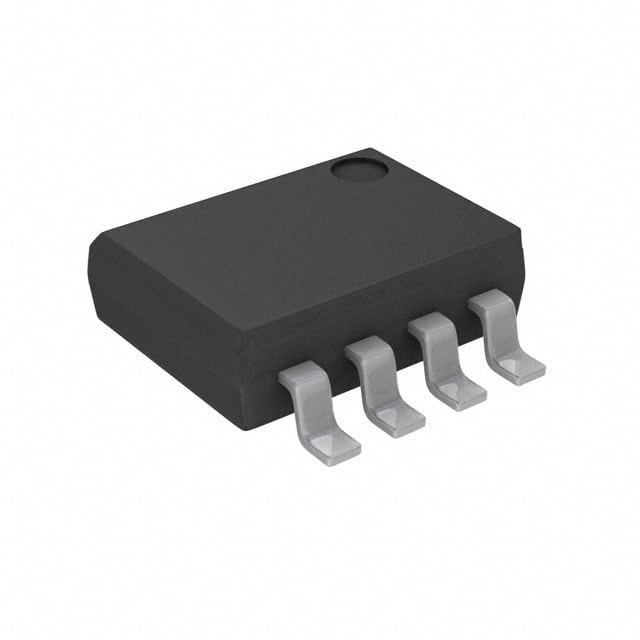
- Package: Surface-mount device (SMD)
- Essence: Non-volatile memory for storing data
- Packaging/Quantity: Varies by manufacturer
Specifications
- Capacity: 32 Megabits (4 Megabytes)
- Interface: Serial Peripheral Interface (SPI)
- Operating Voltage: 2.7V - 3.6V
- Operating Temperature: -40°C to 85°C
- Data Retention: 20 years
- Erase/Program Cycles: 100,000 cycles
Detailed Pin Configuration
The AT25SF321-SSHD-B has a standard SPI interface with the following pin configuration: 1. CS - Chip Select 2. SO - Serial Data Output 3. WP - Write Protect 4. GND - Ground 5. SI - Serial Data Input 6. SCK - Serial Clock 7. HOLD - Hold Input 8. VCC - Power Supply
Functional Features
- High-Speed Read/Write: Enables fast data access and storage
- Low Power Consumption: Suitable for battery-powered devices
- Reliable Data Retention: Ensures long-term storage of critical information
- SPI Interface: Allows for easy integration with microcontrollers and other devices
Advantages and Disadvantages
Advantages
- Fast read/write operations
- Low power consumption
- Reliable data retention
Disadvantages
- Limited erase/program cycles
- Higher cost compared to traditional storage solutions
Working Principles
The AT25SF321-SSHD-B operates on the principle of electrically erasable programmable read-only memory (EEPROM). It utilizes the SPI interface to communicate with the host device, allowing for efficient data transfer and storage.
Detailed Application Field Plans
The AT25SF321-SSHD-B is suitable for a wide range of applications, including: - Consumer electronics - Industrial automation - Automotive systems - Medical devices - Communication equipment
Detailed and Complete Alternative Models
- AT25SF641: Higher capacity variant
- W25Q32JV: Comparable flash memory with different specifications
- MX25L3206E: Alternative from a different manufacturer
In conclusion, the AT25SF321-SSHD-B offers high-speed, reliable data storage for various electronic devices, making it a versatile solution for modern technology applications.
[Word Count: 398]
Enumere 10 preguntas y respuestas comunes relacionadas con la aplicación de AT25SF321-SSHD-B en soluciones técnicas
What is the AT25SF321-SSHD-B?
- The AT25SF321-SSHD-B is a high-speed, SPI-compatible serial flash memory device with 32Mb of memory capacity.
What are the key features of the AT25SF321-SSHD-B?
- The key features include a high-speed clock frequency, low power consumption, flexible erase and program options, and a wide voltage range for compatibility.
How can the AT25SF321-SSHD-B be used in technical solutions?
- It can be used for code storage in embedded systems, firmware updates, configuration storage, boot code storage, and data logging applications.
What are the typical operating conditions for the AT25SF321-SSHD-B?
- The typical operating voltage ranges from 2.7V to 3.6V, and it operates over a wide temperature range, making it suitable for various environments.
What are the programming and erasing options for the AT25SF321-SSHD-B?
- It supports sector and block erase operations, as well as byte and page programming, providing flexibility for different application requirements.
Is the AT25SF321-SSHD-B compatible with standard SPI interfaces?
- Yes, it is fully compatible with standard SPI interfaces, allowing for easy integration into existing designs.
Can the AT25SF321-SSHD-B be used for over-the-air (OTA) firmware updates?
- Yes, its high-speed interface and large memory capacity make it suitable for OTA firmware updates in IoT and connected devices.
What are the power consumption characteristics of the AT25SF321-SSHD-B?
- It has low standby and active power consumption, making it suitable for battery-powered and low-power devices.
Are there any security features available in the AT25SF321-SSHD-B?
- Yes, it offers hardware and software protection features to prevent unauthorized access and ensure data integrity.
What are some common design considerations when using the AT25SF321-SSHD-B?
- Designers should consider signal integrity, layout guidelines, and proper decoupling to ensure reliable operation and performance.