

Consulte las especificaciones para obtener detalles del producto.
AT25XE021A-MHN-T
Introduction
The AT25XE021A-MHN-T is a serial NOR Flash memory device manufactured by Adesto Technologies. This entry provides an overview of the product, including its category, use, characteristics, package, specifications, pin configuration, functional features, advantages and disadvantages, working principles, application field plans, and alternative models.
Basic Information Overview
- Category: Serial NOR Flash Memory
- Use: The AT25XE021A-MHN-T is commonly used in applications that require non-volatile, high-density storage with low power consumption, such as consumer electronics, industrial automation, automotive, and networking devices.
- Characteristics: It offers high-speed read operations, low power consumption, and a wide voltage range for compatibility with various systems.
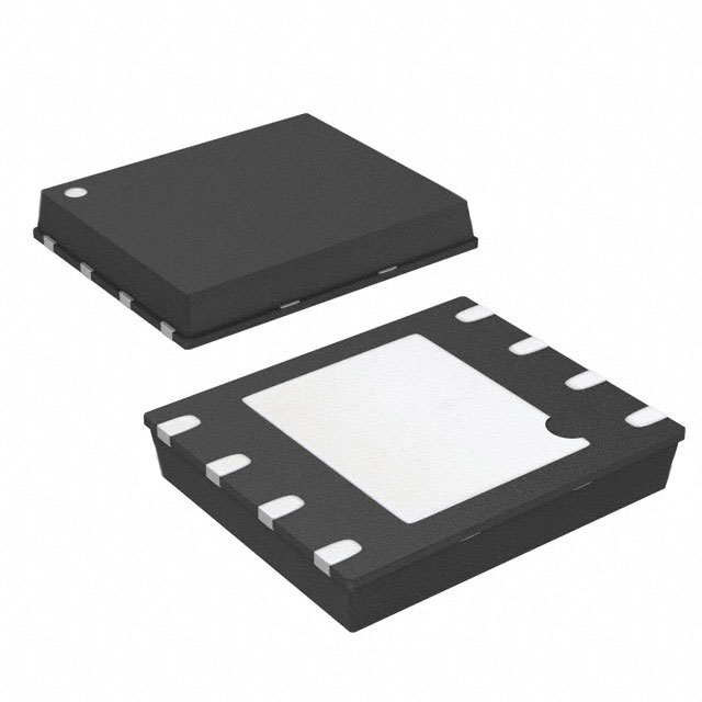
- Package: The AT25XE021A-MHN-T is available in a compact 8-lead SOIC (150-mil) package.
- Essence: The essence of this product lies in its ability to provide reliable, non-volatile memory storage for a wide range of electronic devices.
- Packaging/Quantity: The device is typically supplied in tape and reel packaging with a quantity of 2500 units per reel.
Specifications
- Memory Size: 2Mb (256K x 8)
- Interface: SPI (Serial Peripheral Interface)
- Operating Voltage: 1.7V to 3.6V
- Operating Temperature Range: -40°C to 85°C
- Data Retention: 20 years
- Erase/Program Cycle Endurance: 100,000 cycles
Detailed Pin Configuration
The AT25XE021A-MHN-T features the following pin configuration: 1. /CS (Chip Select) 2. SO (Serial Data Output) 3. WP (Write Protect) 4. GND (Ground) 5. SI (Serial Data Input) 6. SCK (Serial Clock) 7. HOLD (Hold or Reset) 8. VCC (Power Supply)
Functional Features
- High-Speed Read Operations: The device supports fast read operations, enabling quick access to stored data.
- Low Power Consumption: It is designed to minimize power usage, making it suitable for battery-powered applications.
- Flexible Interface: The SPI interface allows for easy integration with various microcontrollers and systems.
Advantages and Disadvantages
Advantages
- High-speed read operations
- Low power consumption
- Wide voltage range compatibility
Disadvantages
- Limited erase/program cycle endurance compared to some competing models
Working Principles
The AT25XE021A-MHN-T utilizes a floating gate technology to store data. When data is written to the memory, charge is trapped in the floating gate, altering the threshold voltage of the memory cell. During read operations, the threshold voltage is measured to determine the stored data.
Detailed Application Field Plans
The AT25XE021A-MHN-T is well-suited for a variety of applications, including: - Consumer Electronics: Smartphones, digital cameras, and portable media players - Industrial Automation: Programmable logic controllers (PLCs) and human-machine interfaces (HMIs) - Automotive: Infotainment systems and engine control units - Networking Devices: Routers, switches, and network attached storage (NAS) systems
Detailed and Complete Alternative Models
Some alternative models to the AT25XE021A-MHN-T include: - Winbond W25Q16JVSSIM - Macronix MX25L1606EMI-12G - Microchip SST26VF032B-104I/MF
In conclusion, the AT25XE021A-MHN-T is a versatile serial NOR Flash memory device with a range of applications and notable features. Its high-speed read operations, low power consumption, and flexible interface make it a compelling choice for designers seeking reliable non-volatile memory solutions.
Word Count: 526
Enumere 10 preguntas y respuestas comunes relacionadas con la aplicación de AT25XE021A-MHN-T en soluciones técnicas
What is the AT25XE021A-MHN-T?
- The AT25XE021A-MHN-T is a serial NOR flash memory device with a capacity of 2 megabits (256K x 8 bits).
What are the key features of the AT25XE021A-MHN-T?
- The key features include a high-speed SPI interface, low power consumption, flexible erase and program capability, and a wide voltage range for compatibility.
What are some typical applications for the AT25XE021A-MHN-T?
- Typical applications include code storage, data storage, parameter storage, and boot code storage in various electronic devices such as IoT devices, consumer electronics, and industrial equipment.
What is the operating voltage range of the AT25XE021A-MHN-T?
- The operating voltage range is from 1.65V to 3.6V, making it suitable for a wide range of applications.
What is the maximum clock frequency supported by the AT25XE021A-MHN-T?
- The maximum clock frequency supported is 104 MHz, enabling high-speed data transfer.
Does the AT25XE021A-MHN-T support software and hardware protection of data?
- Yes, it supports both software and hardware protection of data, providing security for stored information.
What are the temperature ranges for operation and storage of the AT25XE021A-MHN-T?
- The device can operate within a temperature range of -40°C to 85°C and can be stored within a range of -65°C to 150°C.
Is the AT25XE021A-MHN-T RoHS compliant?
- Yes, it is RoHS compliant, meeting environmental standards for electronic components.
What are the package options available for the AT25XE021A-MHN-T?
- The device is available in various package options, including SOIC, WLCSP, and UDFN, offering flexibility for different design requirements.
Are there any evaluation kits or development tools available for the AT25XE021A-MHN-T?
- Yes, there are evaluation kits and development tools available to facilitate the integration and testing of the AT25XE021A-MHN-T in technical solutions.