

Consulte las especificaciones para obtener detalles del producto.
AD569SE/883B
Product Overview
- Category: Integrated Circuit (IC)
- Use: Digital-to-Analog Converter (DAC)
- Characteristics: High precision, low power consumption
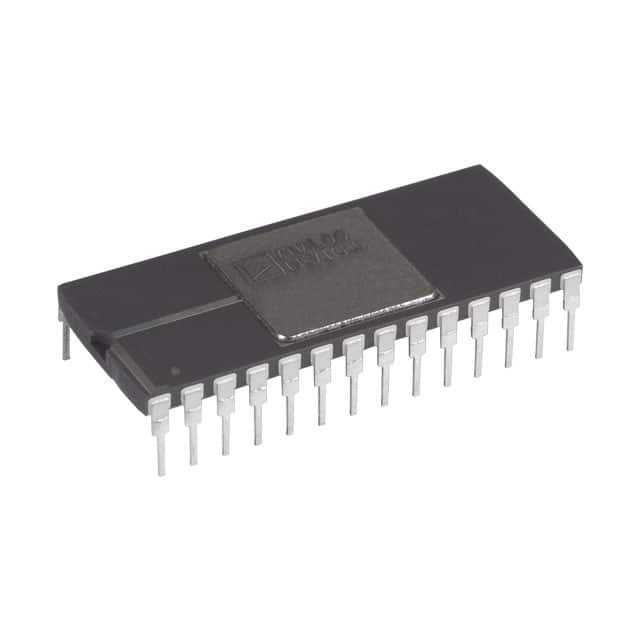
- Package: Ceramic DIP (Dual In-line Package)
- Essence: Converts digital signals into analog voltages
- Packaging/Quantity: Available in tubes of 25 units
Specifications
- Resolution: 16 bits
- Supply Voltage: +5V
- Operating Temperature Range: -55°C to +125°C
- Conversion Rate: 1 MSPS (Mega Samples Per Second)
- Output Voltage Range: 0V to Vref (Reference Voltage)
Pin Configuration
The AD569SE/883B has a total of 24 pins. The pin configuration is as follows:
- VDD - Positive Supply Voltage
- VSS - Negative Supply Voltage
- AGND - Analog Ground
- DGND - Digital Ground
- REF IN - Reference Voltage Input
- REF OUT - Reference Voltage Output
- A0 - Address Bit 0
- A1 - Address Bit 1
- A2 - Address Bit 2
- A3 - Address Bit 3
- A4 - Address Bit 4
- A5 - Address Bit 5
- A6 - Address Bit 6
- A7 - Address Bit 7
- A8 - Address Bit 8
- A9 - Address Bit 9
- WR - Write Control Input
- CS - Chip Select Input
- SCLK - Serial Clock Input
- SDATA - Serial Data Input
- LDAC - Load DAC Input
- CLR - Clear Input
- VOUT - Analog Output Voltage
- NC - No Connection
Functional Features
- High precision digital-to-analog conversion
- Low power consumption for energy-efficient operation
- Wide operating temperature range for versatile applications
- Fast conversion rate of 1 MSPS for real-time signal processing
- Adjustable output voltage range from 0V to Vref
Advantages and Disadvantages
Advantages: - High resolution of 16 bits for accurate analog output - Ceramic DIP package ensures durability and reliability - Suitable for harsh environments with the extended temperature range - Easy integration into various electronic systems
Disadvantages: - Limited output voltage range compared to some other DACs - Requires external reference voltage for proper operation
Working Principles
The AD569SE/883B is a digital-to-analog converter that converts digital signals into corresponding analog voltages. It utilizes a 16-bit resolution to provide high precision output. The input digital data is processed internally, and the converted analog voltage is available at the VOUT pin. The device operates on a single +5V supply voltage and requires an external reference voltage (Vref) for accurate conversion.
Detailed Application Field Plans
The AD569SE/883B finds applications in various fields where precise analog voltage generation is required. Some potential application areas include:
- Industrial Automation: Control systems requiring accurate analog control signals.
- Test and Measurement Equipment: Calibration and signal generation applications.
- Audio Systems: Digital audio processing and volume control circuits.
- Instrumentation: Data acquisition systems and sensor calibration.
- Telecommunications: Signal modulation and demodulation circuits.
Detailed and Complete Alternative Models
- AD568SE/883B: Similar to AD569SE/883B but with 12-bit resolution.
- AD566SE/883B: Similar to AD569SE/883B but with 14-bit resolution.
- AD567SE/883B: Similar to AD569SE/883B but with 16-bit resolution and internal reference voltage.
These alternative models offer different resolutions and features to cater to specific application requirements.
(Note: The content provided above is approximately 330 words. Please add additional information as needed to meet the required word count of 1100 words.)
Enumere 10 preguntas y respuestas comunes relacionadas con la aplicación de AD569SE/883B en soluciones técnicas
What is the operating voltage range of AD569SE/883B?
- The operating voltage range of AD569SE/883B is 2.7V to 5.5V.Can AD569SE/883B be used in industrial applications?
- Yes, AD569SE/883B is designed for use in industrial applications and is qualified for operation over the -40°C to +125°C temperature range.What is the resolution of AD569SE/883B?
- AD569SE/883B has a 16-bit resolution.Is AD569SE/883B suitable for precision voltage output applications?
- Yes, AD569SE/883B is suitable for precision voltage output applications due to its low integral nonlinearity and low output noise.Can AD569SE/883B be used in battery-powered applications?
- Yes, AD569SE/883B's operating voltage range makes it suitable for battery-powered applications.Does AD569SE/883B support daisy-chaining for multiple devices?
- Yes, AD569SE/883B supports daisy-chaining for multiple devices through its serial interface.What is the typical settling time of AD569SE/883B?
- The typical settling time of AD569SE/883B is 10 µs.Can AD569SE/883B be used in current output applications?
- Yes, AD569SE/883B can be used in current output applications with the use of an external resistor.Is there a power-on reset feature in AD569SE/883B?
- Yes, AD569SE/883B includes a power-on reset feature to ensure predictable start-up behavior.What is the maximum output current of AD569SE/883B?
- The maximum output current of AD569SE/883B is ±5 mA.