

Consulte las especificaciones para obtener detalles del producto.
ADN2807ACPZ-RL
Overview
Category
ADN2807ACPZ-RL belongs to the category of integrated circuits (ICs).
Use
It is commonly used in electronic devices for signal processing and communication applications.
Characteristics
- High-performance integrated circuit
- Designed for signal processing and communication purposes
- Compact size and low power consumption
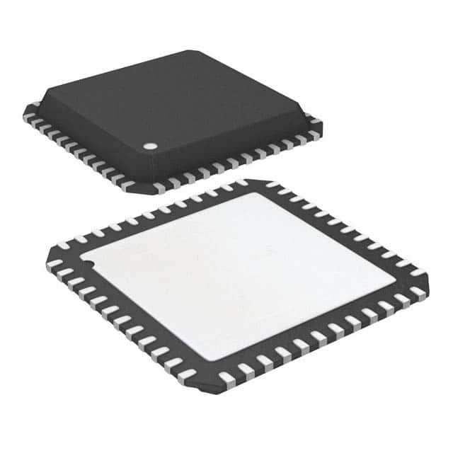
Package
ADN2807ACPZ-RL is available in a small form factor package, typically a leadless chip carrier (LCC) or a plastic ball grid array (PBGA).
Essence
The essence of ADN2807ACPZ-RL lies in its ability to process signals efficiently and accurately, enabling seamless communication in electronic devices.
Packaging/Quantity
This product is usually packaged in reels or trays, with a quantity of 2500 units per reel/tray.
Specifications and Parameters
- Operating Voltage: 3.3V
- Operating Temperature Range: -40°C to +85°C
- Data Rate: Up to 10 Gbps
- Power Consumption: 150mW
- Package Type: LCC or PBGA
Pin Configuration
The pin configuration of ADN2807ACPZ-RL is as follows:
- VCC
- GND
- TXIN
- TXOUT
- RXIN
- RXOUT
- CLK
- RESET
- MODE
Functional Characteristics
ADN2807ACPZ-RL offers the following functional characteristics:
- Signal amplification and conditioning
- Clock recovery and synchronization
- Error detection and correction
- Data encoding and decoding
Advantages and Disadvantages
Advantages
- High-performance signal processing capabilities
- Compact size for space-constrained applications
- Low power consumption for energy efficiency
Disadvantages
- Limited operating temperature range
- Relatively high cost compared to some alternatives
Applicable Range of Products
ADN2807ACPZ-RL is suitable for a wide range of products, including:
- Optical communication systems
- Data center equipment
- High-speed data transmission devices
Working Principles
The working principle of ADN2807ACPZ-RL involves receiving and processing incoming signals, recovering the clock signal, detecting and correcting errors, and encoding/decoding data for reliable transmission.
Detailed Application Field Plans
ADN2807ACPZ-RL can be applied in various fields, such as:
- Fiber-optic communication systems: Enables high-speed data transmission over long distances.
- Networking equipment: Enhances signal processing capabilities for improved network performance.
- Video broadcasting: Facilitates error-free transmission of video signals.
- Telecommunication infrastructure: Supports efficient communication between different network components.
- Industrial automation: Enables reliable data exchange in industrial control systems.
Detailed Alternative Models
Some alternative models to ADN2807ACPZ-RL include:
- ADN2808ACPZ-RL
- ADN2810ACPZ-RL
- ADN2812ACPZ-RL
- ADN2814ACPZ-RL
- ADN2816ACPZ-RL
5 Common Technical Questions and Answers
Q: What is the maximum data rate supported by ADN2807ACPZ-RL? A: ADN2807ACPZ-RL supports data rates up to 10 Gbps.
Q: Can ADN2807ACPZ-RL operate at temperatures below -40°C? A: No, the operating temperature range of ADN2807ACPZ-RL is -40°C to +85°C.
Q: Does ADN2807ACPZ-RL require an external clock signal? A: No, ADN2807ACPZ-RL has built-in clock recovery functionality.
Q: What is the power consumption of ADN2807ACPZ-RL? A: ADN2807ACPZ-RL consumes approximately 150mW of power.
Q: Is ADN2807ACPZ-RL suitable for high-speed data transmission applications? A: Yes, ADN2807ACPZ-RL is designed specifically for high-speed data transmission and communication purposes.
This concludes the encyclopedia entry for ADN2807ACPZ-RL.