

Consulte las especificaciones para obtener detalles del producto.
Encyclopedia Entry: 74AUP1G04FS3-7
Product Overview
- Category: Integrated Circuit (IC)
- Use: Logic Gate Inverter
- Characteristics: Single-gate, low-power, high-speed
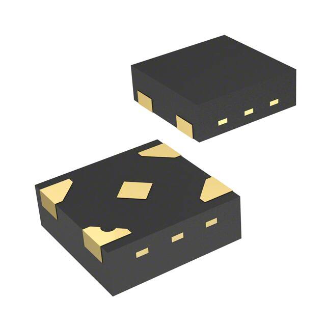
- Package: SOT-353 (SC-88A)
- Essence: The 74AUP1G04FS3-7 is a single-gate logic inverter IC that operates at low power and high speed.
- Packaging/Quantity: Available in tape and reel packaging with 3000 units per reel.
Specifications
- Supply Voltage Range: 0.8V to 3.6V
- Input Voltage Range: 0V to VCC
- Output Voltage Range: 0V to VCC
- Operating Temperature Range: -40°C to +85°C
- Propagation Delay: 2.5 ns (typical) at 3.3V supply voltage
Detailed Pin Configuration
The 74AUP1G04FS3-7 has the following pin configuration:
____
   Y --|    |-- VCC
   A --|    |-- GND
       ----
- Y: Output pin
- A: Input pin
- VCC: Positive power supply
- GND: Ground reference
Functional Features
- Provides logic inversion of the input signal (A) at the output (Y)
- Low power consumption makes it suitable for battery-powered devices
- High-speed operation enables efficient data processing
- Wide supply voltage range allows compatibility with various systems
Advantages and Disadvantages
Advantages: - Low power consumption - High-speed operation - Wide supply voltage range - Small package size
Disadvantages: - Limited functionality as a single-gate inverter - Not suitable for complex logic operations
Working Principles
The 74AUP1G04FS3-7 is based on complementary metal-oxide-semiconductor (CMOS) technology. It utilizes a combination of p-type and n-type MOSFETs to achieve logic inversion. When the input voltage (A) is low, the output voltage (Y) is high, and vice versa.
Detailed Application Field Plans
The 74AUP1G04FS3-7 can be used in various applications, including: 1. Battery-powered devices: Due to its low power consumption, it is ideal for portable electronics such as smartphones, tablets, and wearables. 2. Communication systems: It can be used in signal processing circuits, data transmission, and reception modules. 3. Industrial automation: The IC can be employed in control systems, sensor interfaces, and motor drive circuits. 4. Automotive electronics: It finds application in vehicle control units, infotainment systems, and lighting controls.
Detailed and Complete Alternative Models
Some alternative models that serve similar functions to the 74AUP1G04FS3-7 include: - SN74LVC1G04DBVR - MC74VHC1G04DFT1G - TC7SZ04FU
These alternatives offer comparable features and can be considered based on specific requirements and availability.
In conclusion, the 74AUP1G04FS3-7 is a single-gate logic inverter IC with low power consumption and high-speed operation. Its small package size and wide supply voltage range make it suitable for various applications in battery-powered devices, communication systems, industrial automation, and automotive electronics.
Enumere 10 preguntas y respuestas comunes relacionadas con la aplicación de 74AUP1G04FS3-7 en soluciones técnicas
Sure! Here are 10 common questions and answers related to the application of 74AUP1G04FS3-7 in technical solutions:
Q1: What is the 74AUP1G04FS3-7? A1: The 74AUP1G04FS3-7 is a single inverter gate IC (Integrated Circuit) that is commonly used in digital logic circuits.
Q2: What is the operating voltage range of the 74AUP1G04FS3-7? A2: The operating voltage range of the 74AUP1G04FS3-7 is typically between 0.8V and 3.6V.
Q3: What is the maximum output current of the 74AUP1G04FS3-7? A3: The maximum output current of the 74AUP1G04FS3-7 is around 32mA.
Q4: Can the 74AUP1G04FS3-7 be used as a level shifter? A4: Yes, the 74AUP1G04FS3-7 can be used as a level shifter to convert signals from one voltage level to another.
Q5: What is the propagation delay of the 74AUP1G04FS3-7? A5: The propagation delay of the 74AUP1G04FS3-7 is typically around 2.5ns.
Q6: Can the 74AUP1G04FS3-7 be used in high-speed applications? A6: Yes, the 74AUP1G04FS3-7 is suitable for high-speed applications due to its low propagation delay.
Q7: Is the 74AUP1G04FS3-7 compatible with other logic families? A7: Yes, the 74AUP1G04FS3-7 is compatible with a wide range of logic families, including TTL and CMOS.
Q8: Can the 74AUP1G04FS3-7 be used in battery-powered devices? A8: Yes, the 74AUP1G04FS3-7 is suitable for battery-powered devices due to its low power consumption.
Q9: What is the package type of the 74AUP1G04FS3-7? A9: The 74AUP1G04FS3-7 is available in a small SOT353 package.
Q10: Can the 74AUP1G04FS3-7 be used in automotive applications? A10: Yes, the 74AUP1G04FS3-7 is qualified for automotive applications and can withstand harsh operating conditions.
Please note that the answers provided here are general and may vary depending on specific datasheet specifications and application requirements.