

Consulte las especificaciones para obtener detalles del producto.
Encyclopedia Entry: 74LVC1G126FZ4-7
Product Overview
The 74LVC1G126FZ4-7 is an integrated circuit (IC) belonging to the category of logic gates. It is specifically designed for use in digital electronics applications. This IC is known for its high-speed operation, low power consumption, and compatibility with both 3.3V and 5V systems. The 74LVC1G126FZ4-7 comes in a small package, making it suitable for space-constrained designs. It is commonly used in various electronic devices, such as smartphones, tablets, and portable consumer electronics.
Characteristics
- High-speed operation
- Low power consumption
- Wide voltage compatibility (3.3V and 5V)
- Small package size
Package and Quantity
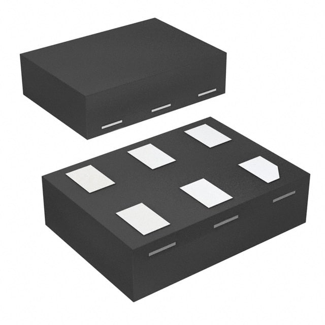
The 74LVC1G126FZ4-7 is available in a surface-mount package. The specific package type is SOT-953 (also known as SC-105AA). Each package contains one unit of the IC.
Specifications
- Supply Voltage Range: 1.65V to 5.5V
- Input Voltage Range: -0.5V to VCC + 0.5V
- Output Voltage Range: GND to VCC
- Maximum Operating Frequency: 400 MHz
- Maximum Propagation Delay: 2.8 ns
- Maximum Quiescent Current: 10 μA
Pin Configuration
The 74LVC1G126FZ4-7 has a total of five pins, which are labeled as follows:
____
   OE --|    |-- VCC
   A  --|    |-- Y
  GND --|    |-- B
       --|____|-- NC
- OE: Output Enable (active low)
- A: Input A
- Y: Output Y
- GND: Ground
- B: Input B
- NC: No Connection
Functional Features
The 74LVC1G126FZ4-7 is a non-inverting buffer with an output enable function. It provides a high-speed, low-power solution for signal buffering and level shifting applications. The output enable pin allows the user to control the output state, enabling or disabling the signal transmission. This feature is particularly useful in reducing power consumption and managing bus contention in multi-device systems.
Advantages and Disadvantages
Advantages
- High-speed operation enables efficient data transmission.
- Low power consumption prolongs battery life in portable devices.
- Wide voltage compatibility allows for versatile integration into different systems.
- Small package size saves valuable board space.
Disadvantages
- Limited number of input/output pins restricts complex circuit designs.
- Lack of built-in protection features may require additional external components for robustness.
Working Principles
The 74LVC1G126FZ4-7 operates based on CMOS (Complementary Metal-Oxide-Semiconductor) technology. It utilizes MOSFET transistors to achieve high-speed switching and low power consumption. When the output enable pin (OE) is active low (logic 0), the input signal at pin A is buffered and transmitted to the output pin Y. Conversely, when the OE pin is inactive high (logic 1), the output is disabled, and the input signal does not pass through.
Application Field Plans
The 74LVC1G126FZ4-7 finds extensive application in various digital electronics domains, including but not limited to: - Mobile devices: smartphones, tablets, wearables - Portable consumer electronics: MP3 players, digital cameras - Computer peripherals: USB interfaces, memory card readers - Industrial automation: sensor interfaces, control systems - Automotive electronics: infotainment systems, driver assistance
Alternative Models
For users seeking alternative options to the 74LVC1G126FZ4-7, several similar ICs are available in the market. These include: - SN74LVC1G126DBVR - MC74VHC1G126DTT1G - TC7SZ126FU
These alternatives offer comparable functionality and characteristics, providing flexibility in design choices.
In conclusion, the 74LVC1G126FZ4-7 is a versatile logic gate IC that combines high-speed operation, low power consumption, and wide voltage compatibility. Its small package size makes it suitable for space-constrained designs. With its functional features and various applications, it serves as an essential component in modern digital electronics systems.
Word Count: 550
Enumere 10 preguntas y respuestas comunes relacionadas con la aplicación de 74LVC1G126FZ4-7 en soluciones técnicas
Sure! Here are 10 common questions and answers related to the application of 74LVC1G126FZ4-7 in technical solutions:
Q1: What is the 74LVC1G126FZ4-7? A1: The 74LVC1G126FZ4-7 is a single bus buffer gate with 3-state output. It is commonly used in digital logic circuits.
Q2: What is the operating voltage range for the 74LVC1G126FZ4-7? A2: The operating voltage range for this IC is typically between 1.65V and 5.5V.
Q3: What is the maximum output current of the 74LVC1G126FZ4-7? A3: The maximum output current is 32mA.
Q4: Can the 74LVC1G126FZ4-7 be used as a level shifter? A4: Yes, it can be used as a level shifter to convert signals from one voltage level to another.
Q5: How many inputs does the 74LVC1G126FZ4-7 have? A5: It has one input.
Q6: How many outputs does the 74LVC1G126FZ4-7 have? A6: It has one output.
Q7: What is the propagation delay of the 74LVC1G126FZ4-7? A7: The typical propagation delay is around 4.3ns.
Q8: Can the 74LVC1G126FZ4-7 be used in high-speed applications? A8: Yes, it is suitable for high-speed applications due to its low propagation delay.
Q9: Is the 74LVC1G126FZ4-7 compatible with other logic families? A9: Yes, it is compatible with both CMOS and TTL logic families.
Q10: Can the 74LVC1G126FZ4-7 be used in battery-powered applications? A10: Yes, it can be used in battery-powered applications as it operates at low voltage levels and has low power consumption.
Please note that these answers are general and may vary depending on specific application requirements.