

Consulte las especificaciones para obtener detalles del producto.
74LVC2G04W6-7
Product Overview
Category
The 74LVC2G04W6-7 belongs to the category of integrated circuits (ICs).
Use
This IC is commonly used as an inverter, which means it can convert a logic level from high to low or vice versa.
Characteristics
- Low-voltage CMOS technology
- High-speed operation
- Wide operating voltage range
- Low power consumption
- Schmitt-trigger input for noise immunity
- Small package size
Package
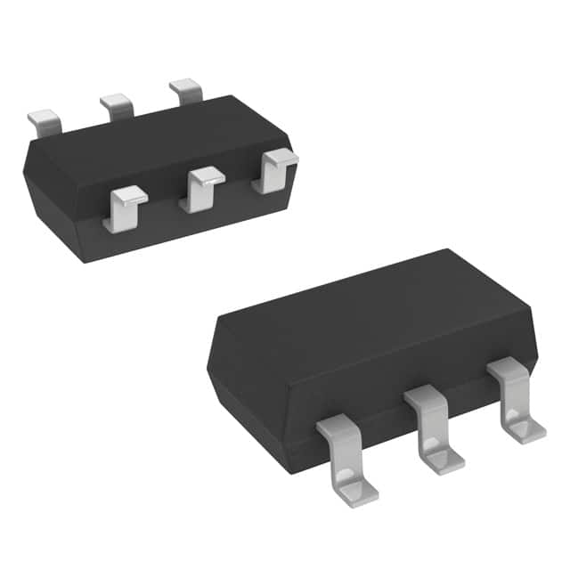
The 74LVC2G04W6-7 is available in a small SOT363 package.
Essence
The essence of this IC lies in its ability to invert logic levels efficiently and reliably.
Packaging/Quantity
The 74LVC2G04W6-7 is typically packaged in reels containing a specific quantity of ICs. The exact quantity may vary depending on the manufacturer's specifications.
Specifications
- Supply Voltage Range: 1.65V to 5.5V
- Input Voltage Range: -0.5V to VCC + 0.5V
- Output Voltage Range: -0.5V to VCC + 0.5V
- Operating Temperature Range: -40°C to +125°C
- Maximum Propagation Delay: 4.3 ns at 3.3V supply voltage
Detailed Pin Configuration
The 74LVC2G04W6-7 has a total of six pins:
- GND: Ground pin
- A: Input pin for logic level
- Y: Output pin for inverted logic level
- A: Input pin for logic level
- Y: Output pin for inverted logic level
- VCC: Power supply pin
Functional Features
- Inverts logic levels: The IC can convert a high logic level to a low logic level and vice versa.
- High-speed operation: It operates at a fast speed, making it suitable for applications requiring quick signal processing.
- Wide operating voltage range: The IC can function within a broad range of supply voltages, providing flexibility in various applications.
- Low power consumption: It consumes minimal power, making it energy-efficient.
- Schmitt-trigger input: This feature enhances noise immunity by providing hysteresis to the input signal.
Advantages and Disadvantages
Advantages
- Compact size: The small package size allows for space-saving designs.
- Versatile application: The IC can be used in a wide range of electronic circuits that require logic level inversion.
- Low power consumption: Its low power consumption makes it suitable for battery-powered devices.
Disadvantages
- Limited output current: The IC has a limited capability to drive heavy loads, which may restrict its use in certain applications.
- Sensitivity to ESD: Like most integrated circuits, the 74LVC2G04W6-7 is sensitive to electrostatic discharge (ESD) and requires proper handling to prevent damage.
Working Principles
The 74LVC2G04W6-7 works based on the principles of complementary metal-oxide-semiconductor (CMOS) technology. It utilizes a combination of NMOS and PMOS transistors to achieve logic level inversion. When the input voltage is high, the PMOS transistor conducts, pulling the output voltage low. Conversely, when the input voltage is low, the NMOS transistor conducts, driving the output voltage high.
Detailed Application Field Plans
The 74LVC2G04W6-7 finds applications in various fields, including:
- Digital electronics: It can be used in digital circuits to invert logic levels and perform signal conditioning.
- Communication systems: The IC can be employed in communication systems to convert logic levels between different components.
- Microcontrollers and microprocessors: It can be utilized in these devices to interface with other components that require inverted logic levels.
- Sensor interfaces: The IC can be used to interface sensors that provide non-inverted logic signals.
Detailed and Complete Alternative Models
Some alternative models to the 74LVC2G04W6-7 include:
- SN74LVC2G04: Manufactured by Texas Instruments, this IC offers similar functionality and characteristics.
- MC74VHC1G04: Produced by ON Semiconductor, this IC is another viable alternative with comparable features.
- NC7SZ04: Manufactured by Fairchild Semiconductor, this IC provides an alternative solution for logic level inversion.
These alternative models can be considered based on specific application requirements and availability.
Word count: 552 words
Enumere 10 preguntas y respuestas comunes relacionadas con la aplicación de 74LVC2G04W6-7 en soluciones técnicas
Sure! Here are 10 common questions and answers related to the application of 74LVC2G04W6-7 in technical solutions:
Q: What is the 74LVC2G04W6-7? A: The 74LVC2G04W6-7 is a dual inverter gate IC, which means it has two inverters in a single package.
Q: What is the voltage supply range for the 74LVC2G04W6-7? A: The voltage supply range for this IC is typically between 1.65V and 5.5V.
Q: What is the maximum output current of the 74LVC2G04W6-7? A: The maximum output current is around 32mA.
Q: Can the 74LVC2G04W6-7 be used as a level shifter? A: Yes, it can be used as a level shifter to convert signals from one voltage level to another.
Q: What is the propagation delay of the 74LVC2G04W6-7? A: The typical propagation delay is around 4.5ns.
Q: Is the 74LVC2G04W6-7 suitable for high-speed applications? A: Yes, it is designed for high-speed operation and can be used in various high-frequency applications.
Q: Can I use the 74LVC2G04W6-7 in battery-powered devices? A: Yes, it has a low power consumption and can be used in battery-powered applications.
Q: Does the 74LVC2G04W6-7 have built-in protection features? A: Yes, it has built-in protection against electrostatic discharge (ESD) and overvoltage.
Q: Can I use the 74LVC2G04W6-7 in both digital and analog circuits? A: Yes, it can be used in both digital and analog applications.
Q: What is the package type of the 74LVC2G04W6-7? A: It comes in a small SOT-363 package, which is suitable for space-constrained designs.
Please note that these answers are general and may vary depending on specific datasheet specifications and application requirements.