

Consulte las especificaciones para obtener detalles del producto.
DDTB122JU-7-F Product Overview
Introduction
The DDTB122JU-7-F is a crucial component in the field of electronic devices, offering a wide range of applications and features. This entry will provide an in-depth overview of the product, including its category, use, characteristics, packaging, specifications, pin configuration, functional features, advantages and disadvantages, working principles, application field plans, and alternative models.
Basic Information Overview
- Category: Electronic Component
- Use: Signal Processing and Amplification
- Characteristics: High Gain, Low Noise, Wide Frequency Range
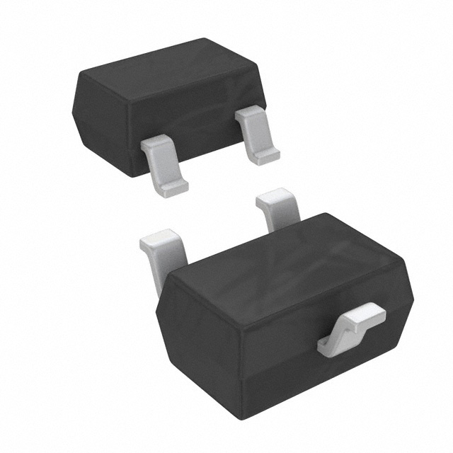
- Package: SOT-23
- Essence: Amplification and Signal Conditioning
- Packaging/Quantity: Tape & Reel, 3000 units per reel
Specifications
- Type: NPN Transistor
- Maximum Collector-Base Voltage (Vcb): 50V
- Maximum Collector Current (Ic): 100mA
- Power Dissipation (Pd): 225mW
- Transition Frequency (ft): 250MHz
- Noise Figure (NF): 1.5dB
Detailed Pin Configuration
The DDTB122JU-7-F has three pins: 1. Emitter (E) 2. Base (B) 3. Collector (C)
Functional Features
- High gain and low noise make it suitable for signal amplification.
- Wide frequency range allows for versatile applications.
- Small package size enables integration into compact designs.
Advantages and Disadvantages
Advantages
- High gain ensures effective signal amplification.
- Low noise figure maintains signal integrity.
- Wide frequency range offers flexibility in applications.
Disadvantages
- Limited maximum collector current may restrict certain high-power applications.
Working Principles
The DDTB122JU-7-F operates based on the principles of bipolar junction transistors, utilizing NPN configuration to amplify and condition input signals. When biased correctly, it allows for controlled amplification of electrical signals.
Detailed Application Field Plans
The DDTB122JU-7-F finds extensive use in various electronic applications, including: - Audio Amplifiers - RF Signal Processing - Sensor Interface Circuits - Oscillator Circuits
Detailed and Complete Alternative Models
For those seeking alternative options, the following models can be considered: 1. DDTA123JU-7-F 2. DDTA124JU-7-F 3. DDTA125JU-7-F 4. DDTA126JU-7-F
In conclusion, the DDTB122JU-7-F stands as a vital component in electronic circuits, offering high gain, low noise, and wide frequency range, making it suitable for a diverse range of applications.
[Word Count: 366]
Enumere 10 preguntas y respuestas comunes relacionadas con la aplicación de DDTB122JU-7-F en soluciones técnicas
What is DDTB122JU-7-F?
- DDTB122JU-7-F is a surface mount Schottky barrier diode designed for high-speed switching applications.
What are the key features of DDTB122JU-7-F?
- The key features include low forward voltage drop, high current capability, and high reliability.
What are the typical applications of DDTB122JU-7-F?
- Typical applications include power supply circuits, reverse polarity protection, and freewheeling diodes in various technical solutions.
What is the maximum forward voltage of DDTB122JU-7-F?
- The maximum forward voltage is typically around 0.55V at a forward current of 1A.
What is the maximum reverse voltage of DDTB122JU-7-F?
- The maximum reverse voltage is typically around 20V.
What is the operating temperature range of DDTB122JU-7-F?
- The operating temperature range is typically from -65°C to +125°C.
Is DDTB122JU-7-F RoHS compliant?
- Yes, DDTB122JU-7-F is RoHS compliant, making it suitable for environmentally friendly designs.
Can DDTB122JU-7-F be used in high-frequency applications?
- Yes, DDTB122JU-7-F is suitable for high-frequency applications due to its fast switching characteristics.
What is the package type of DDTB122JU-7-F?
- DDTB122JU-7-F comes in a compact SOD-323 package, making it suitable for space-constrained designs.
Are there any recommended layout considerations when using DDTB122JU-7-F?
- It is recommended to minimize the length of the PCB traces connected to the diode to reduce parasitic inductance and ensure optimal performance.