

Consulte las especificaciones para obtener detalles del producto.
PI6C49014LIE
Overview
- Category: Integrated Circuit
- Use: Clock Generator and Buffer
- Characteristics: Low power consumption, high performance, compact size
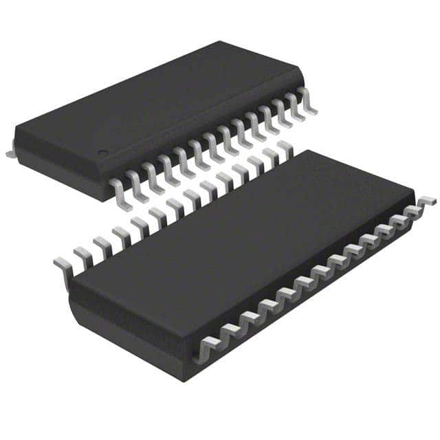
- Package: QFN (Quad Flat No-leads)
- Essence: Clock generation and buffering for electronic devices
- Packaging/Quantity: Tape and Reel, 2500 units per reel
Specifications and Parameters
- Supply Voltage: 1.8V - 3.3V
- Output Frequency Range: 10MHz - 200MHz
- Number of Outputs: 4
- Operating Temperature Range: -40°C to +85°C
- Package Dimensions: 4mm x 4mm
Pin Configuration
The PI6C49014LIE has a total of 20 pins. The pin configuration is as follows:
- VDD
- GND
- OUT0
- OUT1
- OUT2
- OUT3
- OE
- SDA
- SCL
- NC
- NC
- NC
- NC
- NC
- NC
- NC
- NC
- NC
- NC
- NC
Functional Characteristics
- Generates stable clock signals with low jitter
- Provides buffering capability for clock distribution
- Supports I2C interface for easy configuration
- Low power consumption for energy-efficient operation
- Compact size for space-constrained applications
Advantages and Disadvantages
Advantages: - High-performance clock generation and buffering - Wide operating voltage range - Small form factor
Disadvantages: - Limited number of outputs (4) - Requires external components for full functionality
Applicable Range of Products
The PI6C49014LIE is suitable for various electronic devices that require clock generation and buffering. It can be used in applications such as:
- Microcontrollers
- Digital signal processors
- Field-programmable gate arrays (FPGAs)
- Communication systems
- Consumer electronics
Working Principles
The PI6C49014LIE operates by receiving an input clock signal and generating multiple output clock signals with the desired frequency and phase relationship. It also provides buffering capability to ensure signal integrity during distribution.
Detailed Application Field Plans
Microcontroller Systems: The PI6C49014LIE can be used to generate and distribute clock signals for precise timing in microcontroller-based systems.
FPGA Development: It is suitable for FPGA development boards, providing stable clock signals for reliable operation and testing.
Communication Systems: The PI6C49014LIE can be utilized in communication systems to synchronize data transmission and reception.
Industrial Automation: Clock generation and buffering are crucial in industrial automation applications, ensuring accurate timing for various processes.
Consumer Electronics: From smart TVs to gaming consoles, the PI6C49014LIE can be integrated into consumer electronic devices that require reliable clock signals.
Detailed Alternative Models
PI6C49015LIE: Similar to PI6C49014LIE but with additional outputs for more versatile clock distribution.
PI6C49016LIE: Offers enhanced performance and features compared to PI6C49014LIE, suitable for demanding applications.
PI6C49017LIE: Provides higher frequency range and advanced configuration options for specialized applications.
PI6C49018LIE: Designed for low-power applications, offering optimized energy efficiency without compromising performance.
PI6C49019LIE: Compact form factor with extended temperature range, ideal for rugged environments.
5 Common Technical Questions and Answers
Q: What is the maximum operating frequency of the PI6C49014LIE? A: The maximum operating frequency is 200MHz.
Q: Can I use the PI6C49014LIE with a 5V power supply? A: No, the PI6C49014LIE requires a supply voltage between 1.8V and 3.3V.
Q: How many outputs does the PI6C49014LIE have? A: It has four outputs.
Q: Is the PI6C49014LIE compatible with I2C interface? A: Yes, it supports the I2C interface for easy configuration.
Q: What is the package size of the PI6C49014LIE? A: The package dimensions are 4mm x 4mm.
[Word Count: 554]