

Consulte las especificaciones para obtener detalles del producto.
ED315 Product Overview
Introduction
The ED315 belongs to the category of electronic components and is widely used in various electronic devices. This entry provides a comprehensive overview of the ED315, including its basic information, specifications, pin configuration, functional features, advantages and disadvantages, working principles, application field plans, and alternative models.
Basic Information Overview
- Category: Electronic component
- Use: The ED315 is commonly used for signal amplification and processing in electronic circuits.
- Characteristics: It is known for its high gain, low noise, and wide frequency response.
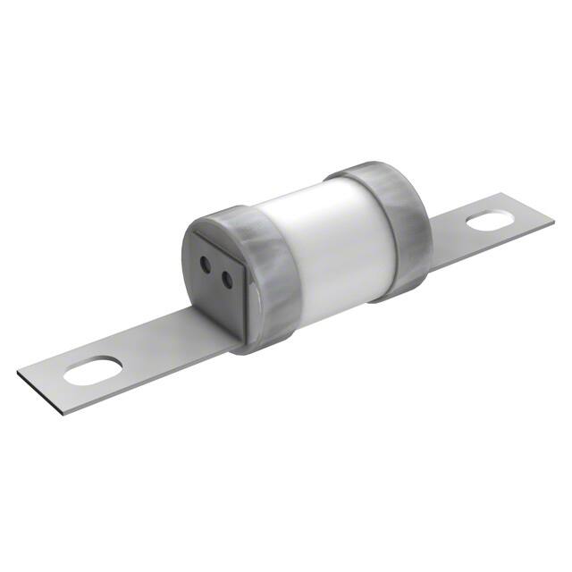
- Package: The ED315 is typically available in a small outline transistor (SOT) package.
- Essence: The essence of the ED315 lies in its ability to amplify weak signals with minimal distortion.
- Packaging/Quantity: It is usually packaged in reels or tubes containing multiple units.
Specifications
The following are the general specifications of the ED315: - Maximum Power Dissipation: 500mW - Collector-Base Voltage (VCBO): 30V - Collector-Emitter Voltage (VCEO): 20V - Emitter-Base Voltage (VEBO): 5V - Collector Current (IC): 100mA - Transition Frequency (fT): 250MHz - Noise Figure: 1.5dB
Detailed Pin Configuration
The ED315 typically has three pins: collector, base, and emitter. The pin configuration is as follows: - Collector (C): Pin 1 - Base (B): Pin 2 - Emitter (E): Pin 3
Functional Features
The key functional features of the ED315 include: - High Gain: The ED315 offers high voltage gain, making it suitable for amplifying weak signals. - Low Noise: It exhibits low noise characteristics, ensuring minimal interference with the input signal. - Wide Frequency Response: The ED315 operates across a broad frequency range, making it versatile for various applications.
Advantages and Disadvantages
Advantages
- High gain for signal amplification
- Low noise performance
- Wide frequency response
- Compact SOT package for space-saving designs
Disadvantages
- Limited maximum power dissipation
- Relatively low collector-emitter voltage rating compared to some alternative models
Working Principles
The ED315 operates based on the principles of bipolar junction transistors (BJTs). When a small signal is applied to the base terminal, it controls the larger current flow between the collector and emitter, effectively amplifying the input signal.
Detailed Application Field Plans
The ED315 finds extensive use in the following application fields: - Audio Amplification: Used in audio amplifiers and preamplifiers to boost weak audio signals. - Radio Frequency (RF) Circuits: Employed in RF amplification stages due to its wide frequency response. - Sensor Interfaces: Integrated into sensor interface circuits to amplify sensor signals for further processing.
Detailed and Complete Alternative Models
Some alternative models to the ED315 include: - ED316: Offers higher collector-emitter voltage rating - ED317: Provides higher maximum power dissipation - ED318: Enhanced noise figure performance for sensitive applications
In conclusion, the ED315 is a versatile electronic component with high gain, low noise, and wide frequency response, making it suitable for various signal amplification applications across different electronic devices.
Word Count: 498
Enumere 10 preguntas y respuestas comunes relacionadas con la aplicación de ED315 en soluciones técnicas
What is ED315?
- ED315 is a common industry standard for electronic devices, specifying requirements for electromagnetic compatibility.
Why is ED315 important in technical solutions?
- ED315 ensures that electronic devices can operate without interfering with each other and without being susceptible to interference from external sources.
How does ED315 impact the design of electronic devices?
- Designers must ensure that their products meet the requirements of ED315 to guarantee electromagnetic compatibility.
What are the key testing procedures involved in ED315 compliance?
- Testing involves evaluating emissions, immunity, and other factors to ensure compliance with ED315 standards.
Are there specific regulations or certifications related to ED315?
- Yes, various regulatory bodies and certification organizations require compliance with ED315 standards for electronic devices.
What are some common challenges in achieving ED315 compliance?
- Common challenges include managing electromagnetic interference, designing for immunity, and meeting strict testing criteria.
How can companies ensure their products meet ED315 requirements?
- Companies can engage in thorough testing, employ experienced engineers, and stay updated on the latest standards and best practices.
What are the consequences of non-compliance with ED315?
- Non-compliance can lead to product failures, legal issues, and damage to a company's reputation.
Are there any emerging trends or developments in ED315 standards?
- Yes, advancements in technology and changes in regulatory requirements continue to influence ED315 standards.
Can ED315 compliance impact international market access?
- Yes, many countries require products to meet ED315 standards for import and sale, making compliance essential for global market access.