

Consulte las especificaciones para obtener detalles del producto.
IPB05CN10N G
Introduction
The IPB05CN10N G is a power MOSFET belonging to the category of electronic components used in various applications. This entry provides an overview of its basic information, specifications, pin configuration, functional features, advantages and disadvantages, working principles, application field plans, and alternative models.
Basic Information Overview
- Category: Power MOSFET
- Use: The IPB05CN10N G is commonly used in power management applications, such as voltage regulation and switching circuits.
- Characteristics: It exhibits low on-state resistance, high switching speed, and efficient power handling capabilities.
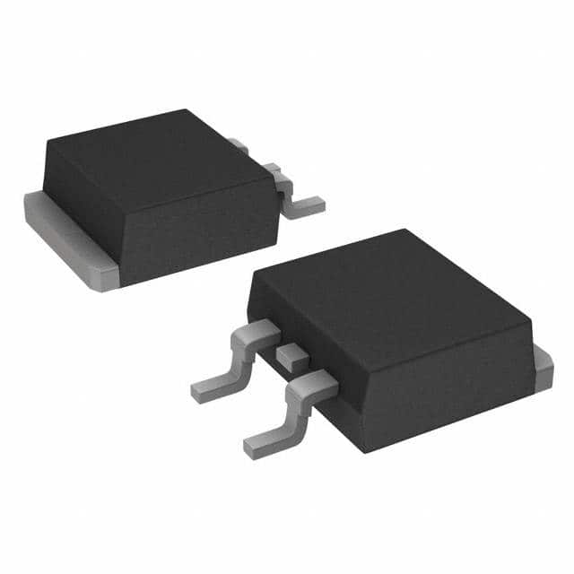
- Package: The IPB05CN10N G is typically available in a TO-263 package.
- Essence: It is designed to provide reliable and efficient power control in various electronic systems.
- Packaging/Quantity: It is usually supplied in reels or tubes containing multiple units.
Specifications
- Voltage Rating: 100V
- Current Rating: 50A
- On-State Resistance: 5.8 mΩ
- Gate Charge: 35nC
- Operating Temperature Range: -55°C to 175°C
- Package Type: TO-263
Detailed Pin Configuration
The IPB05CN10N G typically features three pins: 1. Gate (G): Input for controlling the switching operation. 2. Drain (D): Connection point for the power flow. 3. Source (S): Reference point for the power flow.
Functional Features
- High Efficiency: The MOSFET offers low on-state resistance, minimizing power losses during operation.
- Fast Switching Speed: Enables rapid response in switching applications, contributing to overall system performance.
- Reliable Power Handling: Capable of efficiently managing high currents and voltages.
Advantages and Disadvantages
Advantages
- Efficient power management
- Fast switching capability
- Low on-state resistance
Disadvantages
- Sensitivity to static electricity
- Gate drive considerations required for optimal performance
Working Principles
The IPB05CN10N G operates based on the principle of field-effect transistors, where the gate voltage controls the flow of current between the drain and source terminals. By modulating the gate voltage, the MOSFET can effectively regulate power flow within a circuit.
Detailed Application Field Plans
The IPB05CN10N G finds extensive use in various applications, including: - Voltage regulation in power supplies - Motor control systems - Inverter circuits for renewable energy systems - Switching regulators in electronic devices
Detailed and Complete Alternative Models
- IRF540N
- FDP8870
- STP55NF06L
- IRLB8748
In conclusion, the IPB05CN10N G power MOSFET offers efficient power management and fast switching capabilities, making it suitable for diverse electronic applications. Understanding its specifications, pin configuration, functional features, and application field plans is essential for effective utilization in electronic designs.
[Word Count: 410]
Enumere 10 preguntas y respuestas comunes relacionadas con la aplicación de IPB05CN10N G en soluciones técnicas
What is the IPB05CN10N G?
- The IPB05CN10N G is a power MOSFET transistor designed for use in various technical solutions requiring high efficiency and reliability.
What are the key specifications of the IPB05CN10N G?
- The IPB05CN10N G features a voltage rating of 100V, a continuous drain current of 50A, and low on-resistance for efficient power management.
In what applications can the IPB05CN10N G be used?
- The IPB05CN10N G is commonly used in applications such as motor control, power supplies, and DC-DC converters due to its high performance and robustness.
What are the thermal considerations for using the IPB05CN10N G?
- Proper heat sinking and thermal management are essential when using the IPB05CN10N G to ensure optimal performance and reliability under high-power operation.
Does the IPB05CN10N G require any special driving circuitry?
- The IPB05CN10N G may benefit from gate driver circuits to ensure fast switching and minimize power losses, especially in high-frequency applications.
Are there any recommended layout considerations for implementing the IPB05CN10N G in a PCB design?
- It is advisable to follow recommended PCB layout guidelines to minimize parasitic effects and optimize the performance of the IPB05CN10N G in the circuit.
What protection features does the IPB05CN10N G offer?
- The IPB05CN10N G may include built-in protection against overcurrent, overvoltage, and thermal overload to enhance system reliability and safety.
Can the IPB05CN10N G be used in automotive applications?
- Yes, the IPB05CN10N G is suitable for automotive applications, provided it meets the required automotive-grade standards and qualifications.
How does the IPB05CN10N G compare to similar MOSFET transistors in the market?
- The IPB05CN10N G offers competitive performance, efficiency, and reliability compared to other MOSFET transistors in its class, making it a popular choice for technical solutions.
Where can I find detailed application notes and reference designs for using the IPB05CN10N G?
- Detailed application notes and reference designs for the IPB05CN10N G can be found on the manufacturer's website or through authorized distributors, providing valuable insights into its implementation in technical solutions.