

Consulte las especificaciones para obtener detalles del producto.
SPI08N50C3XKSA1
Introduction
The SPI08N50C3XKSA1 is a power MOSFET belonging to the category of semiconductor devices. This entry provides an overview of its basic information, specifications, pin configuration, functional features, advantages and disadvantages, working principles, application field plans, and alternative models.
Basic Information Overview
- Category: Power MOSFET
- Use: The SPI08N50C3XKSA1 is used as a high-voltage switch in various electronic circuits and power applications.
- Characteristics: It exhibits low on-state resistance, high switching speed, and low gate charge, making it suitable for efficient power management.
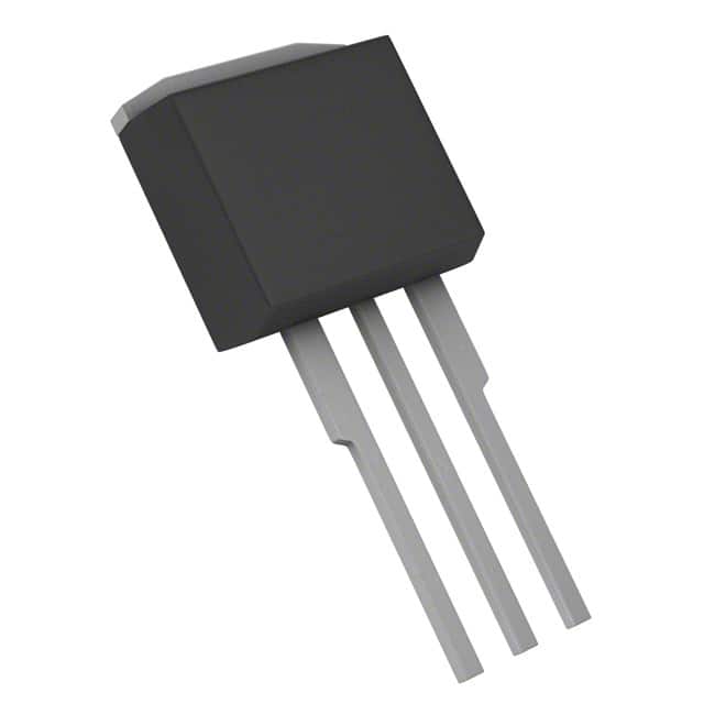
- Package: The SPI08N50C3XKSA1 is typically available in a TO-220 package, providing thermal efficiency and ease of mounting.
- Essence: It serves as a crucial component in power electronics, enabling efficient control and regulation of electrical power.
- Packaging/Quantity: It is commonly supplied in reels or tubes, with quantities varying based on manufacturer specifications.
Specifications
- Voltage Rating: 500V
- Current Rating: 8A
- On-State Resistance: 0.65Ω
- Gate-Source Voltage (Max): ±20V
- Power Dissipation: 125W
- Operating Temperature Range: -55°C to 150°C
Detailed Pin Configuration
The SPI08N50C3XKSA1 typically features a standard pin configuration with three pins: 1. Gate (G): Input terminal for controlling the switching operation. 2. Drain (D): Output terminal connected to the load or power supply. 3. Source (S): Common terminal and reference point for the input and output circuits.
Functional Features
- High Voltage Capability: Enables operation in high-voltage applications.
- Low On-State Resistance: Minimizes power losses and enhances efficiency.
- Fast Switching Speed: Facilitates rapid switching operations, suitable for high-frequency applications.
- Enhanced Thermal Performance: The TO-220 package ensures effective heat dissipation.
Advantages and Disadvantages
Advantages
- Efficient power management
- High voltage capability
- Low on-state resistance
Disadvantages
- Sensitivity to overvoltage conditions
- Limited current handling capacity compared to higher-rated devices
Working Principles
The SPI08N50C3XKSA1 operates based on the principle of field-effect transistors, utilizing the control of the gate-source voltage to modulate the flow of current between the drain and source terminals. When the gate-source voltage is applied, the device transitions between its conducting and non-conducting states, allowing precise control of power flow.
Detailed Application Field Plans
The SPI08N50C3XKSA1 finds extensive use in various applications, including: - Switching power supplies - Motor control systems - Lighting ballasts - Audio amplifiers - Renewable energy systems
Detailed and Complete Alternative Models
- SPI08N60C3: A higher voltage variant suitable for elevated voltage requirements.
- SPI07N80C3: Offers lower on-state resistance for enhanced efficiency in specific applications.
- SPI09N40C3: Designed for applications requiring lower current ratings while maintaining high voltage capabilities.
In conclusion, the SPI08N50C3XKSA1 power MOSFET serves as a critical component in power electronics, offering efficient power management and high-voltage capabilities across diverse applications.
Word Count: 498
Enumere 10 preguntas y respuestas comunes relacionadas con la aplicación de SPI08N50C3XKSA1 en soluciones técnicas
What is the maximum drain-source voltage rating of SPI08N50C3XKSA1?
- The maximum drain-source voltage rating of SPI08N50C3XKSA1 is 500V.
What is the continuous drain current rating of SPI08N50C3XKSA1?
- The continuous drain current rating of SPI08N50C3XKSA1 is 8A.
What is the on-state resistance (RDS(on)) of SPI08N50C3XKSA1?
- The on-state resistance (RDS(on)) of SPI08N50C3XKSA1 is typically 0.5 ohms.
What is the gate-source threshold voltage of SPI08N50C3XKSA1?
- The gate-source threshold voltage of SPI08N50C3XKSA1 is typically 2.5V.
What is the power dissipation of SPI08N50C3XKSA1?
- The power dissipation of SPI08N50C3XKSA1 is typically 125W.
What are the recommended operating temperature range for SPI08N50C3XKSA1?
- The recommended operating temperature range for SPI08N50C3XKSA1 is -55°C to 150°C.
Is SPI08N50C3XKSA1 suitable for high-frequency switching applications?
- Yes, SPI08N50C3XKSA1 is suitable for high-frequency switching applications due to its low RDS(on) and fast switching characteristics.
Does SPI08N50C3XKSA1 have built-in protection features?
- SPI08N50C3XKSA1 does not have built-in protection features and may require external circuitry for overcurrent or overvoltage protection.
What are the typical applications for SPI08N50C3XKSA1?
- Typical applications for SPI08N50C3XKSA1 include power supplies, motor control, and lighting ballasts.
Is SPI08N50C3XKSA1 RoHS compliant?
- Yes, SPI08N50C3XKSA1 is RoHS compliant, meaning it meets the Restriction of Hazardous Substances directive.