

Consulte las especificaciones para obtener detalles del producto.
5CSXFC6D6F31C8NES
Product Overview
Category
5CSXFC6D6F31C8NES belongs to the category of Field Programmable Gate Arrays (FPGAs).
Use
This FPGA is designed for high-performance applications that require programmable logic solutions.
Characteristics
- High-speed and low-power consumption
- Flexible and reconfigurable
- Large capacity for complex designs
- Support for various communication protocols
- Integration of multiple functions on a single chip
Package
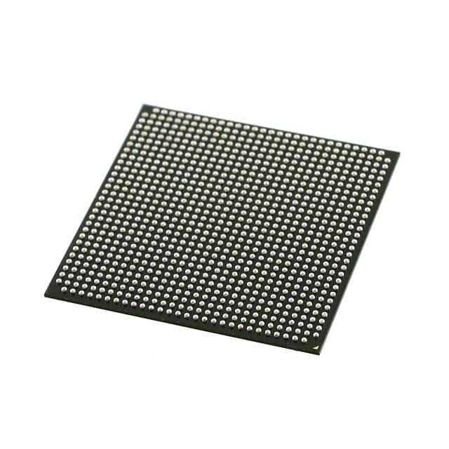
The 5CSXFC6D6F31C8NES FPGA comes in a compact package, suitable for surface mount technology (SMT) assembly.
Essence
The essence of this FPGA lies in its ability to provide customizable digital logic circuits, enabling designers to implement complex functionalities according to their specific requirements.
Packaging/Quantity
Each package contains one 5CSXFC6D6F31C8NES FPGA.
Specifications
- Logic Elements: 6,000
- Embedded Memory: 414 Kbits
- Maximum User I/Os: 266
- DSP Blocks: 24
- Maximum Operating Frequency: 300 MHz
- Configuration Memory: 1,031,040 bits
Detailed Pin Configuration
The 5CSXFC6D6F31C8NES FPGA has a total of 266 user I/O pins. These pins can be configured as inputs or outputs based on the design requirements.
For a detailed pin configuration diagram, please refer to the manufacturer's datasheet.
Functional Features
- High-speed data processing capabilities
- Configurable I/O standards
- On-chip memory resources
- Built-in digital signal processing blocks
- Support for various communication interfaces (e.g., UART, SPI, I2C)
- Reconfigurable logic elements for flexible design implementation
Advantages and Disadvantages
Advantages
- Flexibility in design implementation
- High-performance computing capabilities
- Reduced time-to-market for custom logic solutions
- Lower power consumption compared to traditional ASICs
- Cost-effective for low to medium volume production
Disadvantages
- Steeper learning curve for designers new to FPGA development
- Limited support for high-speed serial interfaces
- Higher cost compared to microcontrollers or standard logic ICs for simple applications
Working Principles
The 5CSXFC6D6F31C8NES FPGA operates based on the principles of reconfigurable digital logic. It consists of configurable logic blocks (CLBs), interconnect resources, embedded memory, and I/O elements. The CLBs can be programmed to implement various logic functions, allowing the FPGA to perform complex computations.
The configuration of the FPGA is stored in non-volatile memory, which is loaded during startup. Once configured, the FPGA executes the desired functionality by routing signals through the programmable interconnect fabric.
Detailed Application Field Plans
The 5CSXFC6D6F31C8NES FPGA finds applications in a wide range of fields, including:
- Telecommunications: Used in base stations, routers, and network switches for high-speed data processing.
- Industrial Automation: Enables control systems for robotics, motor drives, and factory automation.
- Aerospace and Defense: Utilized in radar systems, avionics, and secure communication equipment.
- Medical Devices: Provides customizable solutions for medical imaging, patient monitoring, and diagnostic equipment.
- Automotive: Supports advanced driver assistance systems (ADAS), infotainment systems, and engine control units (ECUs).
Detailed and Complete Alternative Models
- 5CSXFC6D6F31C8N: Similar to 5CSXFC6D6F31C8NES but without the embedded security features.
- 5CSXFC6D6F31C8NE: A lower-cost variant with reduced logic elements and I/O count.
- 5CSXFC6D6F31C8NEX: Enhanced version with additional DSP blocks for increased signal processing capabilities.
These alternative models provide options based on specific project requirements, budget constraints, and desired feature sets.
In conclusion, the 5CSXFC6D6F31C8NES FPGA offers high-performance programmable logic solutions with flexibility, reconfigurability, and integration of multiple functions. Its wide range of applications and availability of alternative models make it a versatile choice for various industries.
Enumere 10 preguntas y respuestas comunes relacionadas con la aplicación de 5CSXFC6D6F31C8NES en soluciones técnicas
Sure! Here are 10 common questions and answers related to the application of 5CSXFC6D6F31C8NES in technical solutions:
Q: What is 5CSXFC6D6F31C8NES? A: 5CSXFC6D6F31C8NES is a specific model number of an FPGA (Field-Programmable Gate Array) manufactured by Intel.
Q: What is an FPGA? A: An FPGA is a type of integrated circuit that can be programmed after manufacturing, allowing for flexible hardware configurations.
Q: What are the typical applications of 5CSXFC6D6F31C8NES? A: 5CSXFC6D6F31C8NES is commonly used in various technical solutions such as industrial automation, telecommunications, automotive systems, and high-performance computing.
Q: How does 5CSXFC6D6F31C8NES differ from other FPGAs? A: 5CSXFC6D6F31C8NES has specific features and capabilities that differentiate it from other FPGAs, such as its logic capacity, I/O capabilities, and performance characteristics.
Q: Can 5CSXFC6D6F31C8NES be reprogrammed multiple times? A: Yes, 5CSXFC6D6F31C8NES is a reprogrammable FPGA, which means it can be reconfigured multiple times to implement different designs or functionalities.
Q: What development tools are available for programming 5CSXFC6D6F31C8NES? A: Intel provides Quartus Prime software suite, which includes design entry, synthesis, simulation, and programming tools specifically tailored for programming 5CSXFC6D6F31C8NES.
Q: Can 5CSXFC6D6F31C8NES interface with other components or devices? A: Yes, 5CSXFC6D6F31C8NES supports various communication protocols and interfaces like PCIe, Ethernet, USB, SPI, I2C, and more, allowing it to interface with other components or devices.
Q: What are the power requirements for 5CSXFC6D6F31C8NES? A: The power requirements for 5CSXFC6D6F31C8NES depend on the specific design and usage scenario. It typically requires a supply voltage of 1.2V and auxiliary voltages for different I/O banks.
Q: Are there any limitations or constraints when using 5CSXFC6D6F31C8NES? A: Like any FPGA, 5CSXFC6D6F31C8NES has certain limitations such as limited logic resources, finite I/O pins, and specific timing constraints that need to be considered during design implementation.
Q: Where can I find additional resources or support for 5CSXFC6D6F31C8NES? A: Intel provides comprehensive documentation, application notes, reference designs, and technical support through their website and community forums for users working with 5CSXFC6D6F31C8NES.