

Consulte las especificaciones para obtener detalles del producto.
HIN232IP
Product Overview
Category
HIN232IP belongs to the category of integrated circuits (ICs).
Use
The HIN232IP is commonly used as a RS-232 interface IC.
Characteristics
- Supports RS-232 voltage levels
- Provides signal conversion between RS-232 and TTL/CMOS logic levels
- Operates with a single power supply
- Offers low power consumption
- Suitable for various communication applications
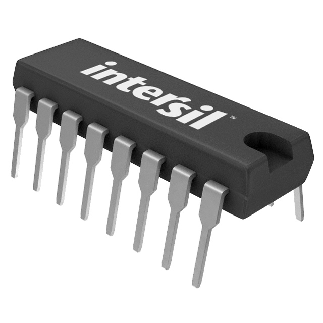
Package
HIN232IP is available in a standard 16-pin DIP (Dual Inline Package) format.
Essence
The essence of HIN232IP lies in its ability to facilitate communication between devices operating at different voltage levels, specifically between RS-232 and TTL/CMOS logic levels.
Packaging/Quantity
HIN232IP is typically packaged in tubes or reels, with quantities varying based on customer requirements.
Specifications
- Supply Voltage: 5V
- Operating Temperature Range: -40°C to +85°C
- Data Rate: Up to 120 kbps
- Number of Channels: 2
- Input/Output Logic Levels: TTL/CMOS
- RS-232 Voltage Levels: ±5V
Detailed Pin Configuration
- VCC - Power supply input
- GND - Ground reference
- T1OUT - Transmitter 1 output
- R1IN - Receiver 1 input
- R1OUT - Receiver 1 output
- T1IN - Transmitter 1 input
- T2IN - Transmitter 2 input
- R2OUT - Receiver 2 output
- R2IN - Receiver 2 input
- T2OUT - Transmitter 2 output
- C1+ - Capacitor 1 positive terminal
- C1- - Capacitor 1 negative terminal
- C2- - Capacitor 2 negative terminal
- C2+ - Capacitor 2 positive terminal
- V- - Negative power supply
- V+ - Positive power supply
Functional Features
- Signal conversion between RS-232 and TTL/CMOS logic levels
- Built-in charge pump for voltage level shifting
- Automatic power shutdown when not in use
- Short-circuit protection on RS-232 outputs
- ESD (Electrostatic Discharge) protection on all pins
Advantages and Disadvantages
Advantages
- Simple integration into existing designs
- Low power consumption
- Wide operating temperature range
- Supports high data rates
- Provides reliable signal conversion
Disadvantages
- Limited to 2 channels
- Requires external capacitors for proper operation
- Not suitable for applications requiring more than 2 channels
Working Principles
HIN232IP utilizes a charge pump circuit to generate the required RS-232 voltage levels from a single power supply. It employs voltage level shifters to convert TTL/CMOS logic levels to RS-232 levels and vice versa. The IC also incorporates automatic power shutdown and protection mechanisms to ensure safe and efficient operation.
Detailed Application Field Plans
HIN232IP finds extensive application in various fields, including but not limited to: - Industrial automation - Telecommunications - Networking equipment - Embedded systems - Consumer electronics
Detailed and Complete Alternative Models
Some alternative models that offer similar functionality to HIN232IP are: - MAX232 - SP232 - LTC1387 - ADM3202
These alternatives can be considered based on specific design requirements and availability.
Word count: 418
Enumere 10 preguntas y respuestas comunes relacionadas con la aplicación de HIN232IP en soluciones técnicas
Sure! Here are 10 common questions and answers related to the application of HIN232IP in technical solutions:
Q: What is HIN232IP? A: HIN232IP is a popular integrated circuit (IC) used for converting RS-232 voltage levels to TTL/CMOS levels and vice versa.
Q: What are the typical applications of HIN232IP? A: HIN232IP is commonly used in various applications such as serial communication, interfacing with microcontrollers, industrial automation, and computer peripherals.
Q: How does HIN232IP convert voltage levels? A: HIN232IP uses charge pumps to generate positive and negative voltages required for RS-232 communication, allowing it to convert between different voltage levels.
Q: What is the operating voltage range of HIN232IP? A: HIN232IP typically operates within a voltage range of +5V to +15V.
Q: Can HIN232IP be used with both TTL and CMOS logic levels? A: Yes, HIN232IP is compatible with both TTL and CMOS logic levels, making it versatile for use with various microcontrollers and devices.
Q: Does HIN232IP require external capacitors? A: Yes, HIN232IP requires external capacitors for proper operation. The datasheet provides recommended values and configurations.
Q: What is the maximum data rate supported by HIN232IP? A: HIN232IP can support data rates up to 120 kbps, making it suitable for most standard serial communication applications.
Q: Can HIN232IP handle multiple RS-232 channels simultaneously? A: Yes, HIN232IP is available in multi-channel versions, allowing it to handle multiple RS-232 channels in a single IC package.
Q: Is HIN232IP immune to electrostatic discharge (ESD)? A: HIN232IP has built-in ESD protection, but additional precautions should be taken to ensure proper ESD protection during handling and installation.
Q: Are there any specific layout considerations for using HIN232IP? A: Yes, the datasheet provides guidelines for PCB layout, including proper grounding, decoupling capacitors, and minimizing noise interference for optimal performance.
Please note that these answers are general and may vary depending on the specific application and requirements. Always refer to the datasheet and consult with technical experts for accurate information.