

Consulte las especificaciones para obtener detalles del producto.
IXTT110N10P
Introduction
The IXTT110N10P is a power MOSFET belonging to the category of electronic components used in various applications. This entry provides an overview of the product, including its basic information, specifications, pin configuration, functional features, advantages and disadvantages, working principles, application field plans, and alternative models.
Basic Information Overview
- Category: Electronic Component
- Use: Power MOSFET for electronic circuits
- Characteristics: High power handling capacity, low on-state resistance, fast switching speed
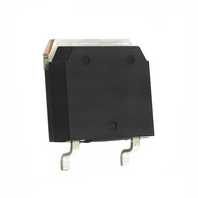
- Package: TO-220AB
- Essence: Efficient power management
- Packaging/Quantity: Typically packaged individually or in reels
Specifications
- Voltage Rating: 100V
- Current Rating: 110A
- On-State Resistance: 4.5mΩ
- Gate Threshold Voltage: 2.0V
- Maximum Power Dissipation: 300W
- Operating Temperature Range: -55°C to 175°C
Detailed Pin Configuration
The IXTT110N10P typically has three pins: 1. Gate (G): Input for controlling the switching of the MOSFET 2. Drain (D): Output terminal for the load 3. Source (S): Common reference terminal
Functional Features
- High current-carrying capability
- Low conduction losses
- Fast switching speed
- Enhanced thermal performance
Advantages and Disadvantages
Advantages
- Efficient power handling
- Low on-state resistance
- Fast switching characteristics
- Suitable for high-power applications
Disadvantages
- Sensitivity to overvoltage conditions
- Gate drive requirements may be more complex compared to other MOSFETs
Working Principles
The IXTT110N10P operates based on the principle of field-effect transistors, where the voltage applied to the gate terminal controls the flow of current between the drain and source terminals. When the gate-source voltage exceeds the threshold, the MOSFET enters the conducting state, allowing current to flow through it.
Detailed Application Field Plans
The IXTT110N10P is commonly used in the following applications: - Switched-mode power supplies - Motor control systems - Inverters and converters - Audio amplifiers - LED lighting systems
Detailed and Complete Alternative Models
Some alternative models to the IXTT110N10P include: - IRFP250N - FDP8878 - STP80NF55-06
In conclusion, the IXTT110N10P is a versatile power MOSFET with high current and voltage ratings, making it suitable for a wide range of electronic applications.
(Word count: 372)
Enumere 10 preguntas y respuestas comunes relacionadas con la aplicación de IXTT110N10P en soluciones técnicas
What is IXTT110N10P?
- IXTT110N10P is a power MOSFET transistor designed for high-speed switching applications in power supplies, motor control, and other electronic systems.
What is the maximum voltage and current rating of IXTT110N10P?
- The maximum voltage rating is 100V, and the maximum continuous drain current is 110A.
What are the typical applications of IXTT110N10P?
- It is commonly used in applications such as motor drives, uninterruptible power supplies (UPS), and welding equipment.
What are the key features of IXTT110N10P that make it suitable for technical solutions?
- Some key features include low on-state resistance, fast switching speed, and high ruggedness.
How does IXTT110N10P contribute to improving efficiency in power supply designs?
- Its low on-state resistance helps minimize power losses and improve overall efficiency in power supply circuits.
What are the thermal considerations when using IXTT110N10P in high-power applications?
- Proper heat sinking and thermal management are crucial to ensure the device operates within its temperature limits and maintains reliability.
Can IXTT110N10P be used in parallel configurations to handle higher currents?
- Yes, it can be paralleled to increase the current-handling capability in high-current applications.
What are the recommended gate drive requirements for IXTT110N10P?
- Adequate gate drive voltage and current must be provided to ensure fast and reliable switching performance.
Are there any specific layout considerations when designing with IXTT110N10P?
- Proper PCB layout, including minimizing parasitic inductance and ensuring good thermal conductivity, is important for optimal performance.
What are the common failure modes associated with IXTT110N10P and how can they be mitigated?
- Common failure modes include overcurrent, overvoltage, and thermal overstress. Proper protection circuits and operating within specified limits can help mitigate these risks.