

Consulte las especificaciones para obtener detalles del producto.
LC4384V-35FT256C
Product Overview
Category: Integrated Circuit (IC)
Use: The LC4384V-35FT256C is a programmable logic device (PLD) that belongs to the family of Complex Programmable Logic Devices (CPLDs). It is designed for digital logic applications and offers high-performance, low-power consumption, and flexibility in circuit design.
Characteristics: - High-density programmable logic device - Low power consumption - Flexible and versatile circuit design capabilities - Fast propagation delay times - Wide operating temperature range
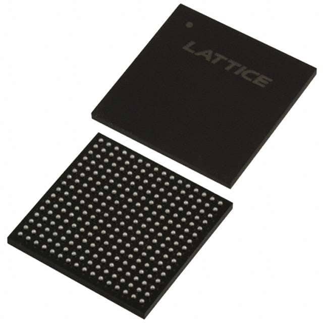
Package: The LC4384V-35FT256C is available in a 256-pin Fine-Pitch Ball Grid Array (FBGA) package. This package provides excellent thermal performance and allows for easy integration into various electronic systems.
Essence: The essence of the LC4384V-35FT256C lies in its ability to provide a highly configurable and reprogrammable logic solution for complex digital designs. It offers a wide range of features and functions that can be tailored to specific application requirements.
Packaging/Quantity: The LC4384V-35FT256C is typically sold individually or in reels, with each reel containing a specified quantity of ICs. The exact packaging and quantity may vary depending on the supplier.
Specifications
- Maximum Operating Frequency: 35 MHz
- Number of Logic Cells: 384
- Number of I/O Pins: 256
- Supply Voltage: 3.3V
- Operating Temperature Range: -40°C to 85°C
Detailed Pin Configuration
The LC4384V-35FT256C has a total of 256 I/O pins, which are organized into different banks. Each bank consists of multiple pins that serve specific functions such as input, output, or bidirectional communication. The detailed pin configuration can be found in the product datasheet provided by the manufacturer.
Functional Features
- High-density programmable logic cells for complex digital designs
- Flexible I/O pin configuration and voltage compatibility
- On-chip memory blocks for data storage
- Dedicated clock management resources for precise timing control
- Built-in security features to protect intellectual property
Advantages and Disadvantages
Advantages: - High-performance and low-power consumption - Versatile and flexible circuit design capabilities - Wide operating temperature range - Secure and reliable operation
Disadvantages: - Limited number of logic cells compared to larger CPLDs or FPGAs - Higher cost compared to simpler logic devices
Working Principles
The LC4384V-35FT256C operates based on the principles of programmable logic. It consists of a matrix of configurable logic cells that can be interconnected to implement various digital functions. The device is programmed using Hardware Description Languages (HDL) such as VHDL or Verilog, which describe the desired logic behavior. Once programmed, the IC performs the specified functions based on the input signals received.
Detailed Application Field Plans
The LC4384V-35FT256C finds applications in various fields where complex digital logic designs are required. Some of the common application areas include:
- Telecommunications: Used in network routers, switches, and communication equipment for signal processing and protocol handling.
- Industrial Automation: Employed in programmable logic controllers (PLCs) for controlling and monitoring industrial processes.
- Automotive Electronics: Integrated into automotive systems for functions like engine control, driver assistance, and infotainment systems.
- Consumer Electronics: Utilized in devices like gaming consoles, set-top boxes, and multimedia players for high-speed data processing and control.
- Medical Devices: Incorporated into medical equipment for data acquisition, signal processing, and control functions.
Detailed and Complete Alternative Models
- LC4128V-75TN100C: A smaller CPLD with 128 logic cells and 100-pin TQFP package.
- LC4064V-75TN44C: Compact CPLD with 64 logic cells and 44-pin TQFP package.
- LC4384V-35FT256I: Similar to LC4384V-35FT256C but with extended temperature range (-40°C to 125°C).
These alternative models offer different combinations of logic cells, I/O pins, and package options to cater to specific design requirements.
Word count: 530 words
Enumere 10 preguntas y respuestas comunes relacionadas con la aplicación de LC4384V-35FT256C en soluciones técnicas
Sure! Here are 10 common questions and answers related to the application of LC4384V-35FT256C in technical solutions:
1. What is LC4384V-35FT256C? - LC4384V-35FT256C is a specific model of Field-Programmable Gate Array (FPGA) manufactured by Lattice Semiconductor.
2. What are the key features of LC4384V-35FT256C? - The key features of LC4384V-35FT256C include 3840 Look-Up Tables (LUTs), 128 Macrocells, 64 I/O pins, and a maximum operating frequency of 35 MHz.
3. What are some typical applications of LC4384V-35FT256C? - LC4384V-35FT256C can be used in various applications such as industrial control systems, automotive electronics, telecommunications, medical devices, and consumer electronics.
4. How can LC4384V-35FT256C be programmed? - LC4384V-35FT256C can be programmed using Hardware Description Languages (HDLs) like VHDL or Verilog, which describe the desired functionality of the FPGA.
5. Can LC4384V-35FT256C be reprogrammed after initial programming? - Yes, LC4384V-35FT256C is a reprogrammable FPGA, allowing for multiple iterations of programming and design changes.
6. What tools are available for programming LC4384V-35FT256C? - Lattice Semiconductor provides software tools like Lattice Diamond or Lattice Radiant, which are commonly used for designing, simulating, and programming FPGAs.
7. What voltage levels does LC4384V-35FT256C support? - LC4384V-35FT256C supports a wide range of voltage levels, including 3.3V, 2.5V, and 1.8V.
8. Can LC4384V-35FT256C interface with other components or devices? - Yes, LC4384V-35FT256C can interface with various components and devices through its I/O pins, allowing for communication with sensors, memory modules, displays, and more.
9. What are the power requirements for LC4384V-35FT256C? - The power requirements for LC4384V-35FT256C typically include a supply voltage of 3.3V and a maximum power consumption of around 500mW.
10. Are there any specific design considerations when using LC4384V-35FT256C? - Some design considerations include proper signal integrity, clock management, power supply decoupling, and thermal management to ensure reliable operation and performance of the FPGA.
Please note that the answers provided here are general and may vary depending on the specific requirements and implementation of the technical solution.