

Consulte las especificaciones para obtener detalles del producto.
LCMXO2-1200HC-6MG132I
Product Overview
Category
The LCMXO2-1200HC-6MG132I belongs to the category of Field-Programmable Gate Arrays (FPGAs).
Use
This FPGA is commonly used in various electronic devices and systems for digital logic implementation, prototyping, and development purposes.
Characteristics
- Low power consumption
- High-performance capabilities
- Small form factor
- Flexible and reprogrammable design
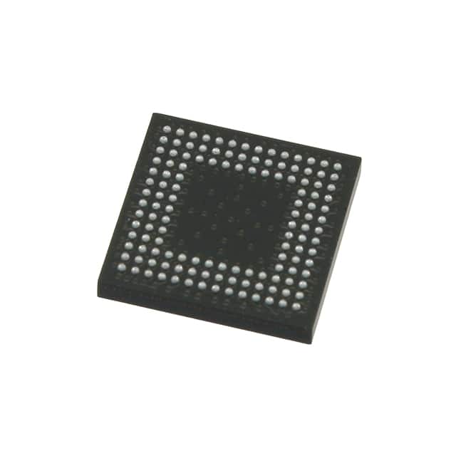
Package
The LCMXO2-1200HC-6MG132I comes in a compact package that ensures easy integration into circuit boards and other electronic systems.
Essence
The essence of this FPGA lies in its ability to provide a customizable hardware platform that allows users to implement complex digital logic functions according to their specific requirements.
Packaging/Quantity
The LCMXO2-1200HC-6MG132I is typically packaged individually and is available in various quantities depending on the manufacturer's specifications.
Specifications
- Model: LCMXO2-1200HC-6MG132I
- Logic Elements: 1200
- Macrocells: 1280
- I/O Pins: 132
- Speed Grade: -6
- Operating Voltage: 1.2V
- Package Type: MG132
Detailed Pin Configuration
The LCMXO2-1200HC-6MG132I has a total of 132 I/O pins, each serving a specific purpose in the overall functionality of the FPGA. The detailed pin configuration can be found in the product datasheet provided by the manufacturer.
Functional Features
- Programmable logic elements for implementing custom digital circuits
- On-chip memory blocks for data storage
- Dedicated input/output pins for interfacing with external devices
- Clock management resources for precise timing control
- Built-in configuration memory for easy reprogramming
Advantages and Disadvantages
Advantages
- Low power consumption, making it suitable for battery-powered devices
- High-performance capabilities enable complex digital logic implementation
- Small form factor allows for space-efficient integration into electronic systems
- Reprogrammable design provides flexibility for iterative development and prototyping
Disadvantages
- Limited resources compared to larger FPGAs, which may restrict the complexity of designs that can be implemented
- Higher cost per logic element compared to other FPGA options
- Steeper learning curve for beginners due to the inherent complexity of FPGA programming
Working Principles
The LCMXO2-1200HC-6MG132I operates based on the principles of configurable logic. It consists of a matrix of programmable logic elements interconnected through configurable routing resources. These logic elements can be programmed to implement various digital functions, such as arithmetic operations, data storage, and control logic. The FPGA's behavior is determined by the configuration data stored in its internal memory, which can be modified by the user.
Detailed Application Field Plans
The LCMXO2-1200HC-6MG132I finds applications in a wide range of fields, including:
- Embedded Systems: Used for implementing custom hardware accelerators, communication interfaces, and control systems.
- Prototyping: Enables rapid prototyping of digital circuits and systems, allowing for quick iterations and design improvements.
- Robotics: Utilized for controlling robot movements, sensor interfacing, and decision-making algorithms.
- Signal Processing: Employed in applications such as audio/video processing, image recognition, and real-time data analysis.
- Internet of Things (IoT): Integrated into IoT devices for data acquisition, processing, and communication.
Detailed and Complete Alternative Models
- LCMXO2-640HC-4SG32C
- LCMXO2-1200HC-4TG100C
- LCMXO2-2000HC-5BG256C
- LCMXO2-4000HC-6TG144C
These alternative models offer varying logic element counts, I/O pin configurations, and package options to cater to different project requirements.
Note: The above information is subject to change based on the manufacturer's specifications and product revisions.
Word Count: 570
Enumere 10 preguntas y respuestas comunes relacionadas con la aplicación de LCMXO2-1200HC-6MG132I en soluciones técnicas
Sure! Here are 10 common questions and answers related to the application of LCMXO2-1200HC-6MG132I in technical solutions:
Q: What is the LCMXO2-1200HC-6MG132I? A: The LCMXO2-1200HC-6MG132I is a low-cost, low-power FPGA (Field-Programmable Gate Array) device manufactured by Lattice Semiconductor.
Q: What are the key features of LCMXO2-1200HC-6MG132I? A: Some key features include 1200 Look-Up Tables (LUTs), 64 Kbits of embedded block RAM, 34 user I/O pins, and support for various I/O standards.
Q: What are some typical applications of LCMXO2-1200HC-6MG132I? A: It can be used in various applications such as industrial automation, consumer electronics, communication systems, medical devices, and more.
Q: How can I program the LCMXO2-1200HC-6MG132I? A: You can program the device using Lattice Diamond design software or iCEcube2 software, which provide a graphical interface for designing and programming the FPGA.
Q: What is the power consumption of LCMXO2-1200HC-6MG132I? A: The power consumption depends on the design and usage, but typically it operates at low power levels, making it suitable for battery-powered applications.
Q: Can I use LCMXO2-1200HC-6MG132I for high-speed applications? A: While it may not be specifically designed for high-speed applications, it can still handle moderate-speed designs and is suitable for many common applications.
Q: Does LCMXO2-1200HC-6MG132I support external memory interfaces? A: Yes, it supports various external memory interfaces such as SPI, I2C, UART, and GPIO, allowing you to interface with external devices or memories.
Q: Can I use LCMXO2-1200HC-6MG132I in a mixed-signal design? A: Yes, you can integrate analog components with the FPGA using external circuitry, making it suitable for mixed-signal applications.
Q: What development boards are available for LCMXO2-1200HC-6MG132I? A: Lattice offers several development boards, such as the iCEstick Evaluation Kit, which provides a low-cost platform for prototyping and evaluation.
Q: Where can I find more resources and support for LCMXO2-1200HC-6MG132I? A: You can visit the Lattice Semiconductor website for datasheets, application notes, user guides, and access to their technical support team.