

Consulte las especificaciones para obtener detalles del producto.
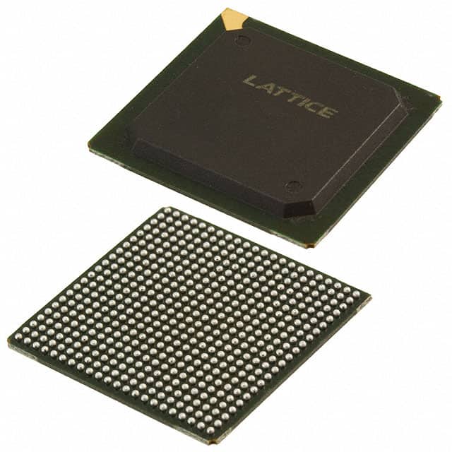
LCMXO2-7000HE-6FG484C
Product Overview
Category
The LCMXO2-7000HE-6FG484C belongs to the category of Field-Programmable Gate Arrays (FPGAs).
Use
FPGAs are integrated circuits that can be programmed and reprogrammed to perform various digital functions. The LCMXO2-7000HE-6FG484C is specifically designed for applications requiring low power consumption and high performance.
Characteristics
- Low power consumption: The LCMXO2-7000HE-6FG484C is optimized for low power operation, making it suitable for battery-powered devices.
- High performance: This FPGA offers fast processing speeds and efficient logic utilization, enabling rapid execution of complex tasks.
- Small package size: The device comes in a compact FG484C package, allowing for space-efficient integration into electronic systems.
- Versatile functionality: With its programmable nature, the LCMXO2-7000HE-6FG484C can be customized to meet specific application requirements.
Package and Quantity
The LCMXO2-7000HE-6FG484C is available in an FG484C package. It is typically sold individually or in small quantities.
Specifications
- Logic Elements: 7,000
- Look-Up Tables (LUTs): 4,500
- Flip-Flops: 9,000
- Block RAM: 270 Kb
- Maximum User I/Os: 211
- Operating Voltage: 1.2V
- Speed Grade: -6
Pin Configuration
The detailed pin configuration of the LCMXO2-7000HE-6FG484C can be found in the manufacturer's datasheet or reference manual.
Functional Features
- Programmability: The LCMXO2-7000HE-6FG484C can be programmed using Hardware Description Languages (HDL) such as VHDL or Verilog, allowing for flexible and customizable functionality.
- Reconfigurability: The FPGA can be reprogrammed multiple times, enabling iterative development and updates to the design without requiring hardware changes.
- I/O Flexibility: The device offers a wide range of user I/Os, allowing for seamless integration with external components and interfaces.
- Low Power Consumption: The LCMXO2-7000HE-6FG484C is designed to minimize power consumption, making it suitable for battery-powered applications.
Advantages and Disadvantages
Advantages
- High performance and fast processing speeds.
- Low power consumption, ideal for energy-efficient designs.
- Versatile functionality and customization options.
- Compact package size for space-constrained applications.
- Reconfigurable nature allows for iterative development.
Disadvantages
- Limited logic elements compared to higher-end FPGAs.
- May require expertise in HDL programming for optimal utilization.
- Higher cost compared to traditional fixed-function integrated circuits.
Working Principles
The LCMXO2-7000HE-6FG484C operates based on the principles of digital logic. It consists of configurable logic blocks, interconnects, and I/O elements. The logic blocks contain Look-Up Tables (LUTs) and flip-flops that can be programmed to implement desired logic functions. The interconnects provide routing paths between different logic blocks, enabling data flow and communication. The I/O elements facilitate interaction with external devices.
Application Field Plans
The LCMXO2-7000HE-6FG484C finds applications in various fields, including but not limited to: 1. Embedded Systems: Used for implementing custom logic in microcontroller-based systems. 2. Communications: Employed in networking equipment for protocol handling and data processing. 3. Industrial Automation: Utilized in control systems for real-time monitoring and decision-making. 4. Consumer Electronics: Integrated into devices like smartphones, tablets, and gaming consoles for enhanced functionality. 5. Internet of Things (IoT): Enables the implementation of custom logic in IoT devices for data processing and connectivity.
Alternative Models
- LCMXO2-1200ZE-1TG144C
- LCMXO2-2000HC-4BG256C
- LCMXO2-4000HE-6BG256C
- LCMXO2-7000HC-4TG144C
These alternative models offer varying specifications and features, catering to different application requirements.
Note: The content provided above is a general structure for an encyclopedia entry and may require further refinement and specific details based on the actual product information.
Enumere 10 preguntas y respuestas comunes relacionadas con la aplicación de LCMXO2-7000HE-6FG484C en soluciones técnicas
Sure! Here are 10 common questions and answers related to the application of LCMXO2-7000HE-6FG484C in technical solutions:
Q: What is the LCMXO2-7000HE-6FG484C? A: The LCMXO2-7000HE-6FG484C is a low-cost, low-power FPGA (Field-Programmable Gate Array) device manufactured by Lattice Semiconductor.
Q: What are the key features of LCMXO2-7000HE-6FG484C? A: Some key features include 7000 Look-Up Tables (LUTs), 128 Kbits of embedded block RAM, 34 I/O pins, and support for various I/O standards.
Q: What are some typical applications of LCMXO2-7000HE-6FG484C? A: It can be used in a wide range of applications such as industrial automation, consumer electronics, communication systems, medical devices, and more.
Q: How can I program the LCMXO2-7000HE-6FG484C? A: You can program the device using Lattice Diamond or Lattice Radiant software tools, which provide a graphical interface for designing and programming the FPGA.
Q: What is the power consumption of LCMXO2-7000HE-6FG484C? A: The power consumption depends on the design and usage, but typically it operates at low power levels, making it suitable for battery-powered applications.
Q: Can I use LCMXO2-7000HE-6FG484C for high-speed applications? A: While it may not be specifically designed for high-speed applications, it can still handle moderate-speed designs and is suitable for many common applications.
Q: Does LCMXO2-7000HE-6FG484C support external memory interfaces? A: Yes, it supports various memory interfaces such as SPI, I2C, and UART, allowing you to interface with external memory devices.
Q: Can I use LCMXO2-7000HE-6FG484C for real-time signal processing? A: Yes, the device has built-in DSP (Digital Signal Processing) blocks that can be used for real-time signal processing tasks.
Q: What development boards are available for LCMXO2-7000HE-6FG484C? A: Lattice offers several development boards, such as the iCEstick Evaluation Kit, which provides a low-cost platform for prototyping and testing designs.
Q: Where can I find more resources and documentation for LCMXO2-7000HE-6FG484C? A: You can visit the Lattice Semiconductor website, where you will find datasheets, application notes, reference designs, and other helpful resources for the device.
Please note that the answers provided here are general and may vary depending on specific requirements and use cases.