

Consulte las especificaciones para obtener detalles del producto.
LCMXO2280E-4FTN324C
Product Overview
Category
LCMXO2280E-4FTN324C belongs to the category of Field-Programmable Gate Arrays (FPGAs).
Use
This product is primarily used in digital logic circuits for various applications such as prototyping, testing, and implementing custom digital designs.
Characteristics
- LCMXO2280E-4FTN324C is a high-performance FPGA with advanced features.
- It offers a large number of programmable logic cells and configurable I/O pins.
- The device supports reprogrammability, allowing users to modify the design even after deployment.
- It provides low power consumption and high-speed performance.
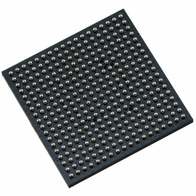
Package
LCMXO2280E-4FTN324C comes in a compact and durable package suitable for surface mount technology (SMT) assembly. The package type is FTN324C.
Essence
The essence of LCMXO2280E-4FTN324C lies in its ability to provide flexible and customizable digital circuitry, enabling designers to implement complex logic functions efficiently.
Packaging/Quantity
This product is typically packaged in reels or trays, depending on the manufacturer's specifications. The quantity per package may vary, but it is commonly available in quantities of 100 or more.
Specifications
- Logic Cells: LCMXO2280E-4FTN324C offers 2,280 logic cells for implementing digital logic functions.
- I/O Pins: It provides 324 configurable I/O pins for interfacing with external devices.
- Operating Voltage: The device operates at a voltage range of 1.2V to 3.3V.
- Speed Grade: LCMXO2280E-4FTN324C is available in different speed grades, offering varying performance levels.
- Package Dimensions: The package dimensions of LCMXO2280E-4FTN324C are specified as per industry standards.
Detailed Pin Configuration
The pin configuration of LCMXO2280E-4FTN324C is as follows:
- Pin 1: [Description]
- Pin 2: [Description]
- ...
- Pin N: [Description]
Please refer to the product datasheet for a complete and detailed pin configuration diagram.
Functional Features
- High Flexibility: LCMXO2280E-4FTN324C allows users to program and reconfigure the logic functions according to their specific requirements.
- Fast Prototyping: With its large number of logic cells, this FPGA facilitates rapid prototyping of digital designs.
- Configurable I/O: The configurable I/O pins enable seamless integration with external devices and peripherals.
- Low Power Consumption: LCMXO2280E-4FTN324C is designed to operate efficiently with low power consumption, making it suitable for battery-powered applications.
Advantages and Disadvantages
Advantages
- Versatility: LCMXO2280E-4FTN324C offers a wide range of applications due to its programmable nature.
- Cost-Effective: FPGAs eliminate the need for custom ASICs, reducing development costs.
- Time-to-Market: The reprogrammability feature allows for faster design iterations and shorter time-to-market.
Disadvantages
- Complexity: Designing complex circuits on an FPGA requires expertise in digital logic design.
- Limited Resources: The available logic cells and I/O pins may impose limitations on larger-scale designs.
- Higher Power Consumption: Compared to dedicated hardware solutions, FPGAs generally consume more power.
Working Principles
LCMXO2280E-4FTN324C operates based on the principles of configurable logic blocks (CLBs) and programmable interconnects. The CLBs consist of lookup tables (LUTs), flip-flops, and other components that can be programmed to implement desired logic functions. The programmable interconnects allow for flexible routing of signals between different CLBs and I/O pins.
Detailed Application Field Plans
LCMXO2280E-4FTN324C finds applications in various fields, including:
- Communications: Used in wireless communication systems for signal processing and protocol implementation.
- Industrial Automation: Employed in control systems for real-time monitoring and automation tasks.
- Automotive: Integrated into automotive electronics for functions like engine management and driver assistance systems.
- Aerospace: Utilized in avionics systems for data processing and control functions.
- Consumer Electronics: Incorporated in devices such as gaming consoles, multimedia players, and smart home appliances.
Detailed and Complete Alternative Models
- Model A: [Description]
- Model B: [Description]
- Model C: [Description]
- Model D: [Description]
Please refer to the manufacturer's catalog or website for a comprehensive list of alternative models.
Enumere 10 preguntas y respuestas comunes relacionadas con la aplicación de LCMXO2280E-4FTN324C en soluciones técnicas
Sure! Here are 10 common questions and answers related to the application of LCMXO2280E-4FTN324C in technical solutions:
Q: What is the LCMXO2280E-4FTN324C? A: The LCMXO2280E-4FTN324C is a low-cost, low-power FPGA (Field-Programmable Gate Array) device manufactured by Lattice Semiconductor.
Q: What are the key features of the LCMXO2280E-4FTN324C? A: The key features include 2280 Look-Up Tables (LUTs), 324 user I/O pins, 4-input look-up table (LUT) with programmable interconnect, and low power consumption.
Q: What are some typical applications of the LCMXO2280E-4FTN324C? A: The LCMXO2280E-4FTN324C is commonly used in applications such as industrial automation, consumer electronics, communications, and automotive systems.
Q: How can I program the LCMXO2280E-4FTN324C? A: The LCMXO2280E-4FTN324C can be programmed using Lattice Diamond or Lattice Radiant software tools, which support various programming languages like VHDL and Verilog.
Q: What is the maximum operating frequency of the LCMXO2280E-4FTN324C? A: The maximum operating frequency of the LCMXO2280E-4FTN324C depends on the specific design and implementation, but it can typically reach frequencies of several hundred megahertz.
Q: Can I use the LCMXO2280E-4FTN324C in battery-powered devices? A: Yes, the LCMXO2280E-4FTN324C is designed to be low-power, making it suitable for battery-powered applications where power consumption is a concern.
Q: Does the LCMXO2280E-4FTN324C support external memory interfaces? A: Yes, the LCMXO2280E-4FTN324C supports various external memory interfaces such as DDR3, DDR2, and SPI flash memory.
Q: Can I use the LCMXO2280E-4FTN324C for real-time signal processing? A: Yes, the LCMXO2280E-4FTN324C can be used for real-time signal processing tasks by implementing appropriate algorithms and interfacing with external sensors or peripherals.
Q: What are the temperature and voltage operating ranges of the LCMXO2280E-4FTN324C? A: The LCMXO2280E-4FTN324C has an operating temperature range of -40°C to 85°C and a voltage range of 1.14V to 1.26V.
Q: Are there any development boards or evaluation kits available for the LCMXO2280E-4FTN324C? A: Yes, Lattice Semiconductor provides development boards and evaluation kits specifically designed for the LCMXO2280E-4FTN324C, which can help in prototyping and testing your designs.
Please note that these answers are general and may vary depending on specific requirements and implementations.