

Consulte las especificaciones para obtener detalles del producto.
LFE5UM-85F-7BG554C
Product Overview
Category
The LFE5UM-85F-7BG554C belongs to the category of Field Programmable Gate Arrays (FPGAs).
Use
This FPGA is commonly used in various electronic devices and systems for digital logic implementation, such as communication equipment, industrial control systems, and consumer electronics.
Characteristics
- High-performance FPGA with advanced programmable logic capabilities.
- Offers a wide range of configurable resources, including Look-Up Tables (LUTs), flip-flops, and embedded memory blocks.
- Provides high-speed interfaces for efficient data transfer.
- Supports complex digital signal processing algorithms.
- Enables rapid prototyping and design iteration.
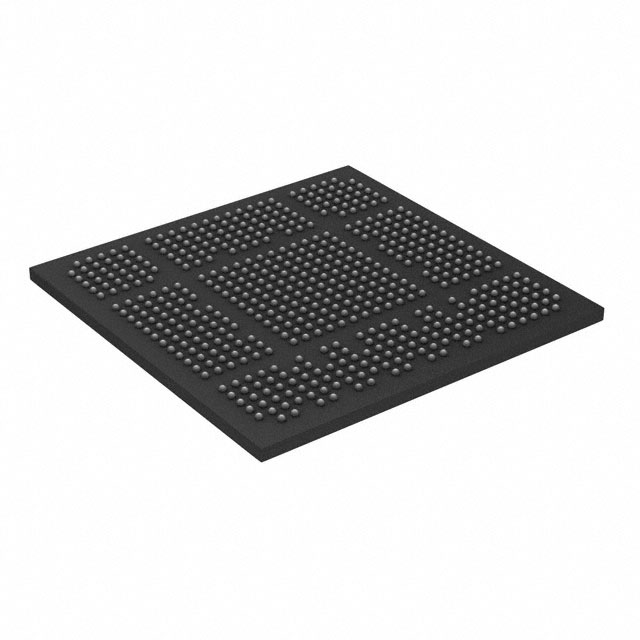
Package
The LFE5UM-85F-7BG554C comes in a compact Ball Grid Array (BGA) package.
Essence
The essence of this FPGA lies in its ability to provide flexible and customizable digital logic functionality, allowing designers to implement complex systems on a single chip.
Packaging/Quantity
Each package contains one LFE5UM-85F-7BG554C FPGA.
Specifications
- Logic Elements: 85,000
- Embedded Memory: 4.8 Mb
- DSP Blocks: 360
- Maximum User I/Os: 554
- Operating Voltage: 1.2V
- Operating Temperature Range: -40°C to 100°C
- Package Type: BGA
- Package Dimensions: 23mm x 23mm
Detailed Pin Configuration
The LFE5UM-85F-7BG554C has a total of 554 user I/O pins, which can be configured for input or output purposes. These pins are distributed across the FPGA package and are labeled according to their respective functions.
For a detailed pin configuration diagram, please refer to the manufacturer's datasheet.
Functional Features
- High-speed data processing capabilities.
- Configurable logic resources for implementing complex digital circuits.
- Support for various communication protocols and interfaces.
- On-chip memory blocks for efficient data storage and retrieval.
- Dedicated Digital Signal Processing (DSP) blocks for performing mathematical operations.
- Built-in clock management resources for precise timing control.
Advantages and Disadvantages
Advantages
- Flexibility: The FPGA can be reprogrammed to adapt to changing design requirements.
- Integration: Multiple functions can be implemented on a single chip, reducing system complexity.
- Rapid Prototyping: FPGAs enable quick design iterations and testing.
- Customizability: Designers have full control over the functionality of the FPGA.
Disadvantages
- Power Consumption: FPGAs tend to consume more power compared to dedicated ASICs.
- Complexity: Designing with FPGAs requires expertise in digital logic design.
- Cost: FPGAs can be more expensive than off-the-shelf integrated circuits for high-volume production.
Working Principles
The LFE5UM-85F-7BG554C operates based on the principles of configurable logic. It consists of an array of programmable logic elements interconnected through configurable routing resources. These logic elements can be programmed to implement desired digital logic functions using Hardware Description Languages (HDLs) such as VHDL or Verilog. Upon programming, the FPGA configures its internal resources to realize the desired functionality.
Detailed Application Field Plans
The LFE5UM-85F-7BG554C finds applications in various fields, including:
- Communication Equipment: Used in network routers, switches, and wireless base stations for high-speed data processing and protocol handling.
- Industrial Control Systems: Employed in automation systems, robotics, and process control applications for real-time control and monitoring.
- Consumer Electronics: Integrated into smart TVs, gaming consoles, and multimedia devices for enhanced processing capabilities and connectivity.
- Medical Devices: Utilized in medical imaging systems, patient monitoring equipment, and diagnostic instruments for data processing and analysis.
Detailed and Complete Alternative Models
- LFE5UM-45F-7BG554C: A lower-cost variant with reduced logic elements but similar features.
- LFE5UM-25F-7BG554C: A compact version with fewer I/O pins, suitable for space-constrained applications.
- LFE5UM-85F-8MG756C: Offers increased embedded memory capacity for data-intensive applications.
These alternative models provide options based on specific project requirements and budget considerations.
Word count: 610 words
Enumere 10 preguntas y respuestas comunes relacionadas con la aplicación de LFE5UM-85F-7BG554C en soluciones técnicas
Sure! Here are 10 common questions and answers related to the application of LFE5UM-85F-7BG554C in technical solutions:
Q: What is the LFE5UM-85F-7BG554C? A: The LFE5UM-85F-7BG554C is a field-programmable gate array (FPGA) manufactured by Lattice Semiconductor.
Q: What are the key features of the LFE5UM-85F-7BG554C? A: The key features include 85,000 logic cells, 554 user I/Os, high-speed transceivers, embedded memory blocks, and low power consumption.
Q: What are some typical applications for the LFE5UM-85F-7BG554C? A: The LFE5UM-85F-7BG554C is commonly used in applications such as telecommunications, industrial automation, automotive electronics, and high-performance computing.
Q: How can I program the LFE5UM-85F-7BG554C? A: The LFE5UM-85F-7BG554C can be programmed using various design tools provided by Lattice Semiconductor, such as Lattice Diamond or Lattice Radiant.
Q: What is the power supply requirement for the LFE5UM-85F-7BG554C? A: The LFE5UM-85F-7BG554C requires a single power supply voltage of 1.2V.
Q: Can I interface the LFE5UM-85F-7BG554C with other devices? A: Yes, the LFE5UM-85F-7BG554C supports various standard interfaces such as SPI, I2C, UART, and GPIOs, allowing easy integration with other devices.
Q: What is the maximum operating frequency of the LFE5UM-85F-7BG554C? A: The LFE5UM-85F-7BG554C can operate at frequencies up to 1 GHz, depending on the design and implementation.
Q: Does the LFE5UM-85F-7BG554C support high-speed serial communication? A: Yes, the LFE5UM-85F-7BG554C has built-in high-speed transceivers that support protocols like PCIe, SATA, USB, and Ethernet.
Q: Can I use the LFE5UM-85F-7BG554C for real-time signal processing? A: Absolutely! The LFE5UM-85F-7BG554C's high logic capacity and embedded memory blocks make it suitable for real-time signal processing applications.
Q: Where can I find additional resources and support for the LFE5UM-85F-7BG554C? A: You can visit Lattice Semiconductor's official website for datasheets, application notes, reference designs, and technical support for the LFE5UM-85F-7BG554C.