

Consulte las especificaciones para obtener detalles del producto.
LT6552CDD#TRPBF
Product Overview
Category
The LT6552CDD#TRPBF belongs to the category of integrated circuits (ICs).
Use
This IC is commonly used in electronic devices for signal conditioning and amplification purposes.
Characteristics
- High-speed operation
- Low power consumption
- Wide input voltage range
- Small package size
- Excellent noise performance
Package
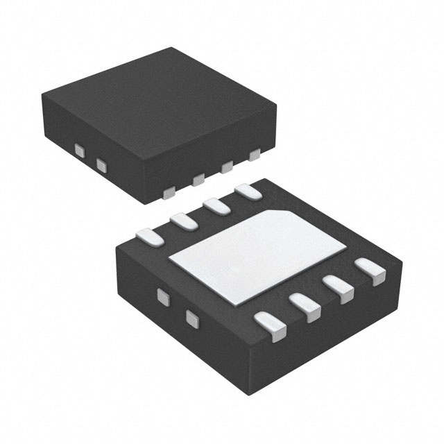
The LT6552CDD#TRPBF is available in a DFN (Dual Flat No-Lead) package.
Essence
The essence of the LT6552CDD#TRPBF is its ability to accurately amplify and condition signals, making it suitable for various applications.
Packaging/Quantity
The LT6552CDD#TRPBF is typically packaged in reels and comes in quantities of 2500 units per reel.
Specifications
- Supply Voltage: 3.3V to 5V
- Bandwidth: 1MHz to 400MHz
- Gain: Adjustable from -6dB to +26dB
- Input Impedance: 100Ω
- Output Impedance: 50Ω
- Operating Temperature Range: -40°C to 85°C
Detailed Pin Configuration
The LT6552CDD#TRPBF has the following pin configuration:
- VCC: Power supply input
- IN-: Negative input terminal
- IN+: Positive input terminal
- GND: Ground
- OUT: Output
Functional Features
- High-speed amplification of input signals
- Adjustable gain control
- Low distortion and noise
- Wide input voltage range
- Stable performance over temperature variations
Advantages and Disadvantages
Advantages
- High-speed operation allows for accurate signal amplification in time-critical applications.
- Wide input voltage range enables compatibility with various signal sources.
- Low power consumption makes it suitable for battery-powered devices.
- Small package size saves board space in compact designs.
- Excellent noise performance ensures clean and reliable signal amplification.
Disadvantages
- Limited gain adjustment range may not be suitable for applications requiring extreme amplification.
- Higher cost compared to some alternative models.
Working Principles
The LT6552CDD#TRPBF operates based on a differential amplifier configuration. It amplifies the difference between the positive and negative input signals, providing a high-gain output signal. The gain can be adjusted using external resistors connected to the gain control pins.
Detailed Application Field Plans
The LT6552CDD#TRPBF finds applications in various fields, including:
- Communication systems: Signal conditioning and amplification in wireless communication devices.
- Test and measurement equipment: Precise signal amplification for accurate measurements.
- Audio systems: Amplification of audio signals in professional audio equipment.
- Medical devices: Signal conditioning in medical imaging and diagnostic equipment.
- Industrial automation: Amplification of sensor signals in control systems.
Detailed and Complete Alternative Models
- AD8001ARZ: High-speed operational amplifier with adjustable gain.
- MAX414CPD: Precision operational amplifier with wide bandwidth.
- LMH6629MA/NOPB: Low-noise, high-speed operational amplifier.
These alternative models offer similar functionality and can be considered as substitutes for the LT6552CDD#TRPBF in specific applications.
Word count: 477 words
Enumere 10 preguntas y respuestas comunes relacionadas con la aplicación de LT6552CDD#TRPBF en soluciones técnicas
Sure! Here are 10 common questions and answers related to the application of LT6552CDD#TRPBF in technical solutions:
Q: What is LT6552CDD#TRPBF? A: LT6552CDD#TRPBF is a high-speed, low-power differential amplifier designed for use in various applications such as video distribution, communications, and instrumentation.
Q: What is the voltage supply range for LT6552CDD#TRPBF? A: The voltage supply range for LT6552CDD#TRPBF is typically between 4.5V and 12V.
Q: What is the bandwidth of LT6552CDD#TRPBF? A: LT6552CDD#TRPBF has a bandwidth of 700MHz, making it suitable for high-frequency signal amplification.
Q: Can LT6552CDD#TRPBF be used in single-ended applications? A: Yes, LT6552CDD#TRPBF can be used in both differential and single-ended applications, providing flexibility in design.
Q: What is the input common-mode range of LT6552CDD#TRPBF? A: The input common-mode range of LT6552CDD#TRPBF extends from -0.5V to +3.5V, allowing for a wide range of input signals.
Q: Does LT6552CDD#TRPBF have built-in gain control? A: No, LT6552CDD#TRPBF does not have built-in gain control. However, external resistors can be used to set the desired gain.
Q: Is LT6552CDD#TRPBF suitable for driving capacitive loads? A: Yes, LT6552CDD#TRPBF is designed to drive capacitive loads up to 100pF without any external compensation.
Q: What is the power consumption of LT6552CDD#TRPBF? A: The power consumption of LT6552CDD#TRPBF is typically around 6.5mA, making it suitable for low-power applications.
Q: Can LT6552CDD#TRPBF operate in high-temperature environments? A: Yes, LT6552CDD#TRPBF can operate in temperatures ranging from -40°C to +85°C, making it suitable for various industrial and automotive applications.
Q: Is LT6552CDD#TRPBF available in different package options? A: Yes, LT6552CDD#TRPBF is available in a 10-lead DFN package, providing compactness and ease of integration into different designs.
Please note that these answers are general and may vary depending on specific datasheet specifications and application requirements.