

Consulte las especificaciones para obtener detalles del producto.
LTC1453CN8#PBF
Product Overview
Category
LTC1453CN8#PBF belongs to the category of integrated circuits (ICs).
Use
This product is commonly used in electronic devices for signal processing and control applications.
Characteristics
- LTC1453CN8#PBF is a high-performance digital-to-analog converter (DAC) IC.
- It offers precise and accurate conversion of digital signals into analog voltages.
- The IC operates at a wide range of supply voltages, making it suitable for various applications.
- It provides low power consumption and high-speed performance.
Package
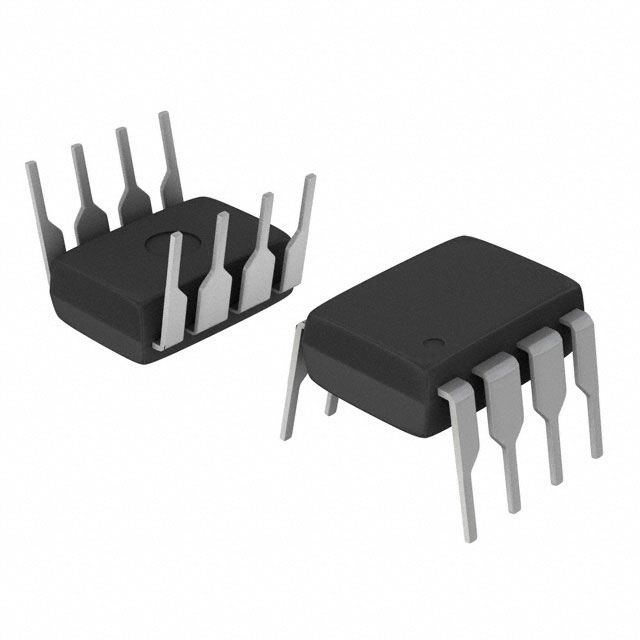
LTC1453CN8#PBF comes in an 8-pin plastic dual in-line package (DIP).
Essence
The essence of LTC1453CN8#PBF lies in its ability to convert digital signals into analog voltages with high precision and efficiency.
Packaging/Quantity
This product is typically packaged in reels or tubes, with a quantity of 250 units per reel/tube.
Specifications
- Resolution: 12 bits
- Supply Voltage Range: 2.7V to 5.5V
- Output Voltage Range: 0V to Vref
- Operating Temperature Range: -40°C to +85°C
- Conversion Time: 10µs (typical)
- Total Unadjusted Error: ±1 LSB (maximum)
Detailed Pin Configuration
LTC1453CN8#PBF features the following pin configuration:
- VDD: Power supply voltage input
- CS: Chip select input
- DIN: Digital input for data
- CLK: Clock input for synchronization
- GND: Ground reference
- VOUT: Analog output voltage
- REF: Reference voltage input
- AGND: Analog ground reference
Functional Features
- High-resolution digital-to-analog conversion
- Wide supply voltage range for versatile applications
- Low power consumption for energy-efficient designs
- Fast conversion time for real-time signal processing
- Accurate and precise analog output voltage
Advantages and Disadvantages
Advantages
- High-performance DAC with 12-bit resolution
- Wide operating voltage range allows compatibility with various systems
- Low power consumption for energy-efficient designs
- Fast conversion time enables real-time signal processing
- Accurate and precise analog output voltage ensures reliable performance
Disadvantages
- Limited output voltage range (0V to Vref)
- Total unadjusted error of ±1 LSB may affect precision in some applications
Working Principles
LTC1453CN8#PBF operates by converting digital input signals into corresponding analog voltages. It utilizes an internal reference voltage (REF) and a clock signal (CLK) to perform the conversion process. The digital data (DIN) is synchronized with the clock signal, and the converted analog voltage is available at the VOUT pin.
Detailed Application Field Plans
LTC1453CN8#PBF finds applications in various fields, including:
- Industrial Automation: Used in control systems for precise analog signal generation.
- Audio Equipment: Employed in audio amplifiers and mixers for accurate volume control.
- Instrumentation: Integrated into measurement devices for generating calibrated analog signals.
- Communication Systems: Utilized in signal processing modules for accurate modulation and demodulation.
- Automotive Electronics: Incorporated in automotive control units for precise sensor calibration.
Detailed and Complete Alternative Models
- LTC1452CN8#PBF: Similar to LTC1453CN8#PBF but with 10-bit resolution.
- LTC1454CN8#PBF: Higher-resolution version with 14-bit DAC capability.
- MAX531BCSD+: Alternative IC with 12-bit resolution and serial interface.
- AD5620BRJZ-2500RL7: 12-bit DAC IC with a smaller package size and lower power consumption.
These alternative models offer similar functionality to LTC1453CN8#PBF but may have different specifications or package options.
Word count: 515 words
Enumere 10 preguntas y respuestas comunes relacionadas con la aplicación de LTC1453CN8#PBF en soluciones técnicas
Sure! Here are 10 common questions and answers related to the application of LTC1453CN8#PBF in technical solutions:
Q: What is LTC1453CN8#PBF? A: LTC1453CN8#PBF is a high-performance, low-power, dual digital-to-analog converter (DAC) designed for various technical applications.
Q: What is the operating voltage range of LTC1453CN8#PBF? A: The operating voltage range of LTC1453CN8#PBF is typically between 2.7V and 5.5V.
Q: What is the resolution of LTC1453CN8#PBF? A: LTC1453CN8#PBF has a resolution of 12 bits, allowing for precise analog output.
Q: Can LTC1453CN8#PBF be used in battery-powered devices? A: Yes, LTC1453CN8#PBF is suitable for battery-powered devices due to its low power consumption.
Q: What is the output voltage range of LTC1453CN8#PBF? A: The output voltage range of LTC1453CN8#PBF is typically between 0V and Vref, where Vref is the reference voltage.
Q: Can LTC1453CN8#PBF be used in industrial control systems? A: Yes, LTC1453CN8#PBF is commonly used in industrial control systems due to its high performance and reliability.
Q: Does LTC1453CN8#PBF support serial communication interfaces? A: Yes, LTC1453CN8#PBF supports both SPI (Serial Peripheral Interface) and I2C (Inter-Integrated Circuit) communication interfaces.
Q: What is the settling time of LTC1453CN8#PBF? A: The settling time of LTC1453CN8#PBF is typically around 10µs, ensuring fast and accurate analog output.
Q: Can LTC1453CN8#PBF be used in automotive applications? A: Yes, LTC1453CN8#PBF is suitable for automotive applications due to its wide operating voltage range and robust design.
Q: Is LTC1453CN8#PBF available in a DIP (Dual In-line Package) form factor? A: Yes, LTC1453CN8#PBF is available in an 8-pin DIP package, making it easy to integrate into various technical solutions.
Please note that these answers are general and may vary depending on specific application requirements.