

Consulte las especificaciones para obtener detalles del producto.
LTC1542IDD#PBF
Product Overview
Category
LTC1542IDD#PBF belongs to the category of integrated circuits (ICs).
Use
This product is commonly used in electronic devices for signal switching and amplification.
Characteristics
- Low power consumption
- High precision
- Wide operating voltage range
- Small package size
Package
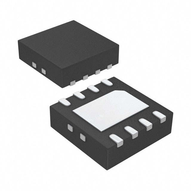
LTC1542IDD#PBF is available in a DFN-8 (Dual Flat No-Lead) package.
Essence
The essence of LTC1542IDD#PBF lies in its ability to efficiently switch and amplify signals with minimal power consumption.
Packaging/Quantity
This product is typically packaged in reels or tubes, with each reel/tube containing a specific quantity of LTC1542IDD#PBF ICs.
Specifications
- Operating Voltage Range: 2.7V to 5.5V
- Supply Current: 50µA (typical)
- Number of Pins: 8
- Input Voltage Range: -0.3V to VCC + 0.3V
- Output Voltage Range: -0.3V to VCC + 0.3V
- Operating Temperature Range: -40°C to 85°C
Detailed Pin Configuration
- GND (Ground)
- IN+ (Positive Input)
- IN- (Negative Input)
- VCC (Power Supply)
- OUT (Output)
- NC (No Connection)
- NC (No Connection)
- SHDN (Shutdown)
Functional Features
- Low quiescent current
- Rail-to-rail input and output operation
- High-speed switching capability
- Shutdown mode for power-saving
Advantages and Disadvantages
Advantages
- Low power consumption extends battery life in portable devices.
- Wide operating voltage range allows compatibility with various power sources.
- Small package size enables space-saving designs.
- High precision ensures accurate signal switching and amplification.
Disadvantages
- Limited number of pins may restrict the complexity of circuit designs.
- Shutdown mode may introduce additional complexity in system control.
Working Principles
LTC1542IDD#PBF operates by receiving input signals through the IN+ and IN- pins. These signals are then amplified and switched based on the desired functionality. The output signal is provided through the OUT pin. The device can be put into a low-power shutdown mode by controlling the SHDN pin.
Detailed Application Field Plans
LTC1542IDD#PBF finds applications in various fields, including but not limited to: - Portable electronic devices - Communication systems - Industrial automation - Medical equipment - Automotive electronics
Detailed and Complete Alternative Models
- LTC1542IMS8#PBF
- LTC1542CMS8#PBF
- LTC1542IS8#PBF
- LTC1542CS8#PBF
- LTC1542CG#PBF
These alternative models offer similar functionality and characteristics to LTC1542IDD#PBF, but may differ in package type or pin configuration.
In conclusion, LTC1542IDD#PBF is an integrated circuit used for signal switching and amplification. Its low power consumption, high precision, and small package size make it suitable for a wide range of applications. However, its limited number of pins and additional complexity introduced by the shutdown mode should be considered.
Enumere 10 preguntas y respuestas comunes relacionadas con la aplicación de LTC1542IDD#PBF en soluciones técnicas
Sure! Here are 10 common questions and answers related to the application of LTC1542IDD#PBF in technical solutions:
Q: What is LTC1542IDD#PBF? A: LTC1542IDD#PBF is a specific model number for a low-power, dual comparator IC (integrated circuit) manufactured by Linear Technology (now part of Analog Devices).
Q: What are the key features of LTC1542IDD#PBF? A: The LTC1542IDD#PBF offers low power consumption, rail-to-rail inputs, and a wide supply voltage range, making it suitable for various applications.
Q: What are some typical applications of LTC1542IDD#PBF? A: LTC1542IDD#PBF can be used in battery-powered systems, portable devices, sensor interfaces, level detection circuits, and general-purpose comparator applications.
Q: What is the operating voltage range for LTC1542IDD#PBF? A: LTC1542IDD#PBF operates from a single supply voltage ranging from 2.7V to 11V.
Q: How much power does LTC1542IDD#PBF consume? A: LTC1542IDD#PBF has a low quiescent current of typically 0.6µA per comparator, making it ideal for low-power applications.
Q: Can LTC1542IDD#PBF handle rail-to-rail input signals? A: Yes, LTC1542IDD#PBF has rail-to-rail input capability, allowing it to accept input signals that span the entire supply voltage range.
Q: What is the output voltage swing of LTC1542IDD#PBF? A: The output voltage swing of LTC1542IDD#PBF is typically within a few millivolts of the supply rails.
Q: Does LTC1542IDD#PBF have built-in hysteresis? A: Yes, LTC1542IDD#PBF features built-in hysteresis, which helps to prevent output oscillation when the input signal is near the threshold voltage.
Q: Can LTC1542IDD#PBF operate in both single-ended and differential mode? A: Yes, LTC1542IDD#PBF can be used in both single-ended and differential mode, providing flexibility in various circuit configurations.
Q: Is LTC1542IDD#PBF available in different package options? A: Yes, LTC1542IDD#PBF is available in an 8-lead DFN (Dual Flat No-Lead) package, which offers small footprint and ease of integration into compact designs.
Please note that the answers provided here are general and may vary depending on specific datasheet specifications and application requirements.