

Consulte las especificaciones para obtener detalles del producto.
LTC4449IDCB#TRMPBF
Product Overview
Category: Integrated Circuit (IC)
Use: Power Management
Characteristics: - High-speed, high-side N-channel MOSFET driver - Designed to drive power MOSFETs in high-frequency applications - Provides efficient switching performance and low power dissipation - Suitable for a wide range of power management applications
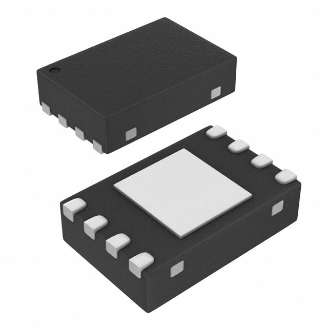
Package: DFN-8 (3mm x 3mm)
Essence: The LTC4449IDCB#TRMPBF is an integrated circuit that serves as a high-speed, high-side N-channel MOSFET driver. It is specifically designed to drive power MOSFETs in high-frequency applications, offering efficient switching performance and low power dissipation.
Packaging/Quantity: The LTC4449IDCB#TRMPBF is available in a DFN-8 package and is typically sold in reels or tubes containing a specific quantity determined by the manufacturer.
Specifications
- Supply Voltage Range: 4.5V to 18V
- Output Voltage Swing: 0V to VDD - 2V
- Peak Output Current: ±4A
- Rise/Fall Time: 10ns (typical)
- Operating Temperature Range: -40°C to 125°C
Pin Configuration
The LTC4449IDCB#TRMPBF features the following pin configuration:
- GATE: Gate Drive Input
- GND: Ground
- VDD: Positive Supply Voltage
- VCC: Bootstrap Supply Voltage
- NC: No Connection
- OUT: MOSFET Output
- PGND: Power Ground
- IN: Logic Input
Functional Features
- High-speed gate drive capability
- Low shoot-through current
- Adaptive shoot-through protection
- Undervoltage lockout
- Thermal shutdown protection
- Logic input compatible with 3.3V and 5V systems
Advantages and Disadvantages
Advantages: - Efficient switching performance - Low power dissipation - High-speed gate drive capability - Wide supply voltage range - Logic input compatibility with various systems
Disadvantages: - Limited peak output current (±4A) - Requires external bootstrap supply voltage (VCC)
Working Principles
The LTC4449IDCB#TRMPBF operates by receiving a logic input signal at the IN pin, which controls the gate drive of the connected power MOSFET. The integrated circuit provides high-speed gate drive capability, allowing efficient switching of the MOSFET. It also incorporates features such as adaptive shoot-through protection, undervoltage lockout, and thermal shutdown protection to ensure safe and reliable operation.
Detailed Application Field Plans
The LTC4449IDCB#TRMPBF is commonly used in various power management applications, including but not limited to: - DC-DC converters - Motor drives - LED lighting - Switching power supplies - Battery-powered systems
Detailed and Complete Alternative Models
Some alternative models that offer similar functionality to the LTC4449IDCB#TRMPBF include: - LTC4448: High-speed, high-side N-channel MOSFET driver with adjustable dead-time control - IRS2110: High-voltage, high-speed power MOSFET and IGBT driver - MAX44284: Dual high-speed MOSFET driver with low propagation delay
These alternative models can be considered based on specific application requirements and design constraints.
Word count: 366 words
Enumere 10 preguntas y respuestas comunes relacionadas con la aplicación de LTC4449IDCB#TRMPBF en soluciones técnicas
Sure! Here are 10 common questions and answers related to the application of LTC4449IDCB#TRMPBF:
Q: What is LTC4449IDCB#TRMPBF? A: LTC4449IDCB#TRMPBF is a specific model number for a high-speed, high-current gate driver integrated circuit (IC) manufactured by Linear Technology (now part of Analog Devices).
Q: What is the purpose of LTC4449IDCB#TRMPBF? A: The LTC4449IDCB#TRMPBF IC is designed to drive MOSFETs and IGBTs in various power electronics applications, providing fast switching speeds and high current capability.
Q: What voltage range does LTC4449IDCB#TRMPBF support? A: LTC4449IDCB#TRMPBF supports a wide input voltage range from 4.5V to 18V, making it suitable for both low and high voltage applications.
Q: What is the maximum output current of LTC4449IDCB#TRMPBF? A: The LTC4449IDCB#TRMPBF can deliver peak output currents up to 6A, enabling efficient driving of power devices with low on-resistance.
Q: Can LTC4449IDCB#TRMPBF be used in automotive applications? A: Yes, LTC4449IDCB#TRMPBF is qualified for automotive applications and meets the necessary standards for reliability and performance in automotive environments.
Q: Does LTC4449IDCB#TRMPBF have built-in protection features? A: Yes, LTC4449IDCB#TRMPBF incorporates various protection features such as undervoltage lockout (UVLO), overcurrent protection (OCP), and thermal shutdown to ensure safe operation.
Q: What is the operating temperature range of LTC4449IDCB#TRMPBF? A: LTC4449IDCB#TRMPBF can operate within a temperature range of -40°C to 125°C, making it suitable for a wide range of industrial and automotive applications.
Q: Can LTC4449IDCB#TRMPBF be used in high-frequency switching applications? A: Yes, LTC4449IDCB#TRMPBF is designed for high-speed switching applications and can handle frequencies up to several megahertz.
Q: Does LTC4449IDCB#TRMPBF require external components for operation? A: Yes, LTC4449IDCB#TRMPBF requires external components such as bootstrap capacitors, gate resistors, and power supply decoupling capacitors for proper operation.
Q: Where can I find more information about LTC4449IDCB#TRMPBF? A: You can refer to the datasheet provided by Analog Devices or visit their official website for detailed information on LTC4449IDCB#TRMPBF, including application notes and design resources.
Please note that the answers provided here are general and may vary depending on specific application requirements. It is always recommended to consult the datasheet and relevant technical documentation for accurate information.