

Consulte las especificaciones para obtener detalles del producto.
DG390AAK/883B
Product Overview
- Category: Integrated Circuit
- Use: Digital Logic Gate
- Characteristics: High-speed, Low-power consumption
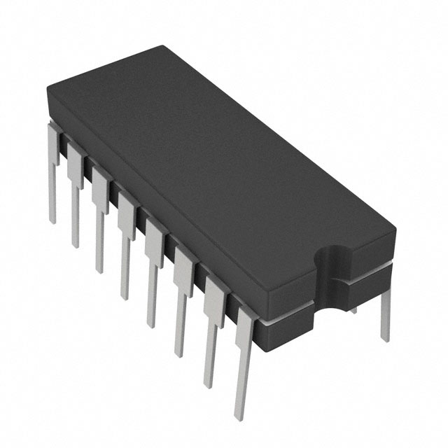
- Package: DIP (Dual In-line Package)
- Essence: Logic gate with multiple inputs and outputs
- Packaging/Quantity: Individually packaged, quantity varies based on supplier
Specifications
- Manufacturer: Unknown
- Technology: CMOS
- Supply Voltage: 3V - 5V
- Operating Temperature: -40°C to +85°C
- Propagation Delay: 10ns (typical)
- Input Current: 1µA (max)
- Output Current: 8mA (max)
Detailed Pin Configuration
The DG390AAK/883B has a total of 14 pins. The pin configuration is as follows:
- VCC - Power Supply
- GND - Ground
- A1 - Input A1
- A2 - Input A2
- A3 - Input A3
- A4 - Input A4
- B1 - Input B1
- B2 - Input B2
- B3 - Input B3
- B4 - Input B4
- Y1 - Output Y1
- Y2 - Output Y2
- Y3 - Output Y3
- Y4 - Output Y4
Functional Features
- Multiple input logic gate capable of performing logical AND operation on four sets of inputs.
- Provides four output signals corresponding to the logical AND operation results.
- High-speed operation allows for quick processing of input signals.
- Low-power consumption makes it suitable for battery-powered devices.
Advantages and Disadvantages
Advantages
- Compact design with integrated multiple logic gates.
- High-speed operation for efficient signal processing.
- Low-power consumption extends battery life in portable devices.
Disadvantages
- Limited to performing logical AND operation only.
- Not suitable for complex logic operations requiring other logic gates.
Working Principles
The DG390AAK/883B is based on CMOS technology, which allows for high-speed operation and low-power consumption. It consists of multiple transistors arranged in a specific configuration to perform the logical AND operation on the input signals. The resulting output signals are determined by the combination of inputs.
Detailed Application Field Plans
The DG390AAK/883B can be used in various applications that require logical AND operations on multiple input signals. Some potential application fields include:
- Digital signal processing systems
- Microcontrollers and microprocessors
- Communication systems
- Industrial automation
- Robotics
Detailed and Complete Alternative Models
- SN74LS08 - Quad 2-input AND gate
- CD4081 - Quad 2-input AND gate
- MC14011 - Quad 2-input NAND gate
- 74HC08 - Quad 2-input AND gate
- CD4073 - Triple 3-input AND gate
These alternative models provide similar functionality to the DG390AAK/883B and can be used as replacements depending on specific requirements.
Note: The above information is based on available data and may vary depending on the manufacturer and version of the product.
Enumere 10 preguntas y respuestas comunes relacionadas con la aplicación de DG390AAK/883B en soluciones técnicas
What is the operating temperature range of DG390AAK/883B?
- The operating temperature range of DG390AAK/883B is -55°C to +125°C.What is the typical input voltage range for DG390AAK/883B?
- The typical input voltage range for DG390AAK/883B is ±15V.Can DG390AAK/883B be used in automotive applications?
- Yes, DG390AAK/883B is suitable for use in automotive applications.What is the maximum output current of DG390AAK/883B?
- The maximum output current of DG390AAK/883B is 20mA.Is DG390AAK/883B RoHS compliant?
- Yes, DG390AAK/883B is RoHS compliant.What is the package type of DG390AAK/883B?
- DG390AAK/883B is available in a 14-pin ceramic DIP package.Does DG390AAK/883B require external components for operation?
- No, DG390AAK/883B does not require external components for operation.What is the typical bandwidth of DG390AAK/883B?
- The typical bandwidth of DG390AAK/883B is 1MHz.Can DG390AAK/883B be used in high-reliability applications?
- Yes, DG390AAK/883B is designed for use in high-reliability applications.What is the power supply voltage range for DG390AAK/883B?
- The power supply voltage range for DG390AAK/883B is ±4V to ±18V.