

Consulte las especificaciones para obtener detalles del producto.
MAX5442ACUB+T
Product Overview
Category
MAX5442ACUB+T belongs to the category of integrated circuits (ICs).
Use
This product is commonly used in electronic devices for digital-to-analog conversion.
Characteristics
- High precision and accuracy
- Low power consumption
- Wide operating voltage range
- Small package size
- Easy integration into various electronic systems
Package
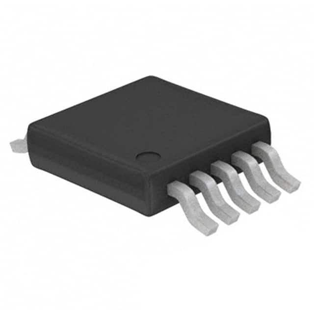
The MAX5442ACUB+T is available in a small 10-pin µMAX package.
Essence
The essence of MAX5442ACUB+T lies in its ability to convert digital signals into analog voltages with high precision and accuracy.
Packaging/Quantity
This product is typically packaged in reels or tubes, with a quantity of 2500 units per reel/tube.
Specifications
- Resolution: 12 bits
- Operating Voltage Range: 2.7V to 5.5V
- Output Voltage Range: 0V to VDD
- Power Consumption: 1.5mW (typical)
- Operating Temperature Range: -40°C to +85°C
Detailed Pin Configuration
- VDD: Power supply voltage input
- GND: Ground reference
- DIN: Digital input for data transfer
- CS: Chip select input
- SCLK: Serial clock input
- LDAC: Load DAC input
- REFOUT: Reference voltage output
- AGND: Analog ground reference
- OUT: Analog output voltage
- NC: No connection
Functional Features
- High-resolution digital-to-analog conversion
- Serial interface for easy integration with microcontrollers
- Internal reference voltage generation
- Power-down mode for reduced power consumption
- Fast settling time for rapid response
Advantages and Disadvantages
Advantages
- High precision and accuracy in digital-to-analog conversion
- Low power consumption for energy-efficient designs
- Wide operating voltage range allows compatibility with various systems
- Small package size enables space-saving integration
Disadvantages
- Limited output voltage range (0V to VDD)
- Requires external components for proper operation
- Relatively higher cost compared to lower-resolution DACs
Working Principles
The MAX5442ACUB+T operates by accepting digital input data through the DIN pin. This data is then converted into an analog voltage based on the resolution of the device. The internal reference voltage ensures accurate conversion, and the output voltage is available at the OUT pin. The chip select (CS) and serial clock (SCLK) inputs control the data transfer process. The load DAC (LDAC) input allows for simultaneous updating of multiple DAC outputs.
Detailed Application Field Plans
The MAX5442ACUB+T finds applications in various fields, including:
- Audio Equipment: Used for volume control, tone adjustment, and audio signal processing.
- Industrial Automation: Provides precise analog control signals for motor speed control, valve positioning, and sensor calibration.
- Test and Measurement Instruments: Enables accurate signal generation and calibration in oscilloscopes, function generators, and data acquisition systems.
- Communication Systems: Used for modulation, demodulation, and signal conditioning in wireless communication devices.
- Automotive Electronics: Provides analog control signals for automotive systems such as climate control, lighting, and engine management.
Detailed and Complete Alternative Models
- MAX5312BCPD+: 12-bit digital-to-analog converter with similar specifications and package options.
- LTC1668CGN#PBF: 16-bit digital-to-analog converter with extended resolution and wider temperature range.
- MCP4922-E/P: 12-bit dual-channel digital-to-analog converter with SPI interface and low power consumption.
These alternative models offer similar functionality and can be considered based on specific application requirements.
In conclusion, the MAX5442ACUB+T is a high-precision digital-to-analog converter with various advantages such as low power consumption, wide operating voltage range, and small package size. It finds applications in audio equipment, industrial automation, test and measurement instruments, communication systems, and automotive electronics. Alternative models like MAX5312BCPD+, LTC1668CGN#PBF, and MCP4922-E/P provide additional options for different design needs.
Enumere 10 preguntas y respuestas comunes relacionadas con la aplicación de MAX5442ACUB+T en soluciones técnicas
Sure! Here are 10 common questions and answers related to the application of MAX5442ACUB+T:
Q: What is the MAX5442ACUB+T? A: The MAX5442ACUB+T is a digital-to-analog converter (DAC) IC that converts digital signals into analog voltages.
Q: What is the operating voltage range of the MAX5442ACUB+T? A: The MAX5442ACUB+T operates from a single supply voltage ranging from 2.7V to 5.5V.
Q: How many bits of resolution does the MAX5442ACUB+T have? A: The MAX5442ACUB+T has 12 bits of resolution, allowing for precise control over the analog output voltage.
Q: What is the maximum output voltage range of the MAX5442ACUB+T? A: The MAX5442ACUB+T can provide an output voltage range of 0V to Vref, where Vref is the reference voltage supplied to the DAC.
Q: Can the MAX5442ACUB+T be used in both single-ended and differential output configurations? A: Yes, the MAX5442ACUB+T can be configured for both single-ended and differential output modes, providing flexibility in various applications.
Q: What is the typical settling time of the MAX5442ACUB+T? A: The typical settling time of the MAX5442ACUB+T is 10µs, ensuring fast response and accurate output voltage transitions.
Q: Does the MAX5442ACUB+T have any built-in power-on reset circuitry? A: Yes, the MAX5442ACUB+T features a power-on reset circuit that ensures the DAC output is set to zero during power-up.
Q: Can the MAX5442ACUB+T operate in a low-power mode? A: Yes, the MAX5442ACUB+T has a low-power mode that reduces the power consumption when not actively converting digital signals.
Q: What is the maximum operating temperature range of the MAX5442ACUB+T? A: The MAX5442ACUB+T can operate within a temperature range of -40°C to +85°C.
Q: Are there any evaluation boards or development kits available for the MAX5442ACUB+T? A: Yes, Maxim Integrated provides evaluation kits and reference designs that can help users quickly prototype and evaluate the MAX5442ACUB+T in their applications.
Please note that these answers are general and may vary depending on specific application requirements and datasheet specifications.