

Consulte las especificaciones para obtener detalles del producto.
MAX6389XS33D1+T
Product Overview
- Category: Integrated Circuit (IC)
- Use: Voltage Regulator
- Characteristics: Low Dropout, Precision, Adjustable Output
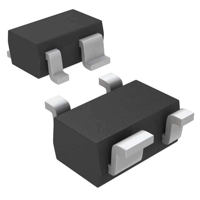
- Package: SOT23-5
- Essence: This IC is a low dropout voltage regulator designed to provide a stable and adjustable output voltage for various applications.
- Packaging/Quantity: Tape and Reel, 3000 units per reel
Specifications
- Input Voltage Range: 2.5V to 6.5V
- Output Voltage Range: 1.25V to 5.5V
- Dropout Voltage: 120mV at 100mA load current
- Output Current: Up to 150mA
- Line Regulation: ±0.05% typical
- Load Regulation: ±0.1% typical
- Quiescent Current: 50µA typical
- Operating Temperature Range: -40°C to +85°C
Detailed Pin Configuration
The MAX6389XS33D1+T IC has the following pin configuration:
- GND: Ground connection
- FB: Feedback pin for adjusting the output voltage
- EN: Enable pin for turning the regulator on/off
- BYP: Bypass capacitor connection for improved stability
- VOUT: Output voltage pin
Functional Features
- Low dropout voltage allows operation with small input-output differentials
- Adjustable output voltage provides flexibility for various applications
- Excellent line and load regulation ensures stable output voltage under varying conditions
- Low quiescent current minimizes power consumption in standby mode
- Thermal shutdown and current limit protection for enhanced reliability
Advantages and Disadvantages
Advantages: - Wide input voltage range allows compatibility with different power sources - Adjustable output voltage provides versatility for various applications - Low dropout voltage enables efficient operation with small input-output differentials - Excellent line and load regulation ensures stable output voltage under varying conditions
Disadvantages: - Limited output current capability (up to 150mA) - SOT23-5 package may require surface mount soldering expertise
Working Principles
The MAX6389XS33D1+T is a low dropout voltage regulator that uses a PNP pass transistor to regulate the output voltage. It operates by comparing the feedback voltage (FB) with an internal reference voltage, and adjusts the pass transistor accordingly to maintain a stable output voltage. The enable pin (EN) allows the regulator to be turned on or off, conserving power when not needed. The bypass capacitor (BYP) improves stability by filtering out high-frequency noise.
Detailed Application Field Plans
The MAX6389XS33D1+T can be used in various applications where a stable and adjustable output voltage is required. Some potential application fields include:
- Battery-powered devices: Provides a regulated voltage for microcontrollers, sensors, and other low-power components.
- Portable audio devices: Ensures a stable voltage supply for audio amplifiers, DACs, and headphone drivers.
- Industrial control systems: Regulates voltage for analog and digital circuitry in control panels, PLCs, and motor drives.
- Automotive electronics: Supplies a reliable voltage for automotive sensors, lighting systems, and infotainment modules.
- IoT devices: Enables stable voltage for wireless communication modules, sensors, and microcontrollers in IoT applications.
Detailed and Complete Alternative Models
- LM1117-3.3: Low dropout voltage regulator with fixed 3.3V output voltage. Available in various packages.
- LT1763-3.3: Low dropout voltage regulator with fixed 3.3V output voltage. Offers high PSRR and low noise performance.
- MCP1702-3302E: Low dropout voltage regulator with fixed 3.3V output voltage. Provides low quiescent current and thermal shutdown protection.
These alternative models offer similar functionality to the MAX6389XS33D1+T, but with different specifications and package options.
Note: The content provided above is a sample structure for an encyclopedia entry and may not reflect actual information about the MAX6389XS33D1+T or its alternatives.
Enumere 10 preguntas y respuestas comunes relacionadas con la aplicación de MAX6389XS33D1+T en soluciones técnicas
Sure! Here are 10 common questions and answers related to the application of MAX6389XS33D1+T in technical solutions:
Q1: What is MAX6389XS33D1+T? A1: MAX6389XS33D1+T is a voltage reference IC manufactured by Maxim Integrated. It provides a stable and accurate voltage reference of 3.3V.
Q2: What is the typical application of MAX6389XS33D1+T? A2: The typical application of MAX6389XS33D1+T includes providing a stable voltage reference for various electronic circuits, such as microcontrollers, ADCs, DACs, and sensors.
Q3: What is the operating voltage range of MAX6389XS33D1+T? A3: The operating voltage range of MAX6389XS33D1+T is from 2.7V to 5.5V.
Q4: What is the output voltage accuracy of MAX6389XS33D1+T? A4: The output voltage accuracy of MAX6389XS33D1+T is typically ±0.5%.
Q5: Can MAX6389XS33D1+T provide a stable output voltage under varying load conditions? A5: Yes, MAX6389XS33D1+T has excellent load regulation characteristics, ensuring a stable output voltage even with varying loads.
Q6: Does MAX6389XS33D1+T require any external components for operation? A6: No, MAX6389XS33D1+T is a standalone voltage reference IC and does not require any external components for operation.
Q7: What is the temperature coefficient of MAX6389XS33D1+T? A7: The temperature coefficient of MAX6389XS33D1+T is typically 50ppm/°C.
Q8: Can MAX6389XS33D1+T operate in harsh environmental conditions? A8: Yes, MAX6389XS33D1+T is designed to operate in a wide temperature range of -40°C to +125°C, making it suitable for harsh environments.
Q9: What is the output current capability of MAX6389XS33D1+T? A9: The output current capability of MAX6389XS33D1+T is typically 20mA.
Q10: Is MAX6389XS33D1+T available in different package options? A10: Yes, MAX6389XS33D1+T is available in a SOT23-3 package, which is small and easy to integrate into various circuit designs.
Please note that these answers are general and may vary depending on the specific datasheet and application requirements.