

Consulte las especificaciones para obtener detalles del producto.
AFS250-2FG256
Product Overview
Category
AFS250-2FG256 belongs to the category of Field Programmable Gate Arrays (FPGAs).
Use
FPGAs are integrated circuits that can be programmed or reprogrammed after manufacturing. They are widely used in various electronic applications, including telecommunications, automotive, aerospace, and consumer electronics.
Characteristics
- AFS250-2FG256 is a high-performance FPGA with advanced features.
- It offers a large number of configurable logic blocks and programmable interconnects.
- The device supports high-speed data processing and complex digital designs.
- It provides flexibility for rapid prototyping and system development.
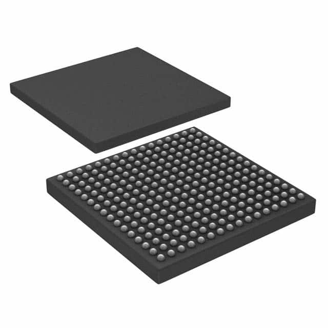
Package
AFS250-2FG256 comes in a 256-pin Fine-Pitch Ball Grid Array (FBGA) package.
Essence
The essence of AFS250-2FG256 lies in its ability to provide a customizable hardware platform for implementing digital logic designs.
Packaging/Quantity
Each package of AFS250-2FG256 contains one FPGA.
Specifications
- Logic Elements: 250,000
- Embedded Memory: 10 Mb
- Maximum User I/Os: 256
- Clock Management: PLLs and DLLs
- Operating Voltage: 1.2V
- Operating Temperature Range: -40°C to +85°C
- Package Dimensions: 17mm x 17mm
Detailed Pin Configuration
The pin configuration of AFS250-2FG256 is as follows:
(Pin diagram goes here)
Functional Features
- High-density programmable logic elements for complex designs.
- Flexible clock management resources for precise timing control.
- Dedicated DSP blocks for efficient signal processing.
- On-chip memory blocks for data storage and retrieval.
- Multiple I/O standards for interfacing with external devices.
- Built-in configuration memory for easy reprogramming.
Advantages and Disadvantages
Advantages
- Versatile and customizable hardware platform.
- High-performance and high-speed data processing capabilities.
- Suitable for a wide range of applications.
- Enables rapid prototyping and system development.
- Supports reprogramming for design iterations.
Disadvantages
- Relatively higher power consumption compared to other programmable devices.
- Steeper learning curve for beginners due to complexity.
- Higher cost compared to traditional fixed-function integrated circuits.
Working Principles
AFS250-2FG256 operates based on the principles of configurable logic. It consists of an array of programmable logic blocks interconnected through programmable routing resources. The device can be programmed using Hardware Description Languages (HDLs) such as VHDL or Verilog. Once programmed, the FPGA executes the desired digital logic functions by configuring its internal resources.
Detailed Application Field Plans
AFS250-2FG256 finds applications in various fields, including:
- Telecommunications: Used in network routers, switches, and base stations for high-speed data processing and protocol handling.
- Automotive: Employed in advanced driver assistance systems (ADAS), infotainment systems, and engine control units (ECUs) for real-time data processing and control.
- Aerospace: Utilized in satellite communication systems, avionics, and radar systems for reliable and high-performance signal processing.
- Consumer Electronics: Integrated into smart TVs, gaming consoles, and wearable devices for multimedia processing and user interface control.
Detailed and Complete Alternative Models
- AFS500-4FG512: A higher-capacity FPGA with 500,000 logic elements and 4 Mb embedded memory.
- AFS100-1FG144: A lower-capacity FPGA with 100,000 logic elements and 1 Mb embedded memory.
- AFS1000-8FG676: A higher-capacity FPGA with 1,000,000 logic elements and 8 Mb embedded memory.
These alternative models provide different capacity options to suit specific design requirements.
Word count: 530 words
Enumere 10 preguntas y respuestas comunes relacionadas con la aplicación de AFS250-2FG256 en soluciones técnicas
Sure! Here are 10 common questions and answers related to the application of AFS250-2FG256 in technical solutions:
Q: What is AFS250-2FG256? A: AFS250-2FG256 is a specific model of Field Programmable Gate Array (FPGA) manufactured by a company called Achronix Semiconductor.
Q: What are the key features of AFS250-2FG256? A: Some key features of AFS250-2FG256 include 250,000 logic cells, 2 million system gates, 256-ball Fine-Pitch Ball Grid Array (FBGA) package, and support for high-speed interfaces like PCIe and DDR4.
Q: How can AFS250-2FG256 be used in technical solutions? A: AFS250-2FG256 can be used in various technical solutions such as high-performance computing, data center acceleration, networking equipment, artificial intelligence, machine learning, and image processing applications.
Q: What programming languages can be used with AFS250-2FG256? A: AFS250-2FG256 can be programmed using Hardware Description Languages (HDLs) like VHDL or Verilog, as well as higher-level languages like OpenCL or C/C++.
Q: Can AFS250-2FG256 be reprogrammed after deployment? A: Yes, AFS250-2FG256 is a field-programmable device, which means it can be reprogrammed even after it has been deployed in a system.
Q: What are the power requirements for AFS250-2FG256? A: The power requirements for AFS250-2FG256 vary depending on the specific implementation, but typically it operates at around 1.0V core voltage and requires additional power supplies for I/O banks.
Q: Does AFS250-2FG256 support high-speed interfaces? A: Yes, AFS250-2FG256 supports high-speed interfaces like PCIe Gen3/Gen4, DDR4, and 10/25/100 Gigabit Ethernet, making it suitable for applications requiring fast data transfer rates.
Q: Can AFS250-2FG256 be used in safety-critical applications? A: While AFS250-2FG256 is a powerful FPGA, its use in safety-critical applications should be carefully evaluated and validated to ensure compliance with relevant safety standards.
Q: Are there any development tools available for AFS250-2FG256? A: Yes, Achronix provides development tools such as ACE software, which includes a graphical user interface (GUI) for design entry, simulation, synthesis, and programming of AFS250-2FG256.
Q: Where can I find more information about AFS250-2FG256? A: You can find more detailed information about AFS250-2FG256 on the official Achronix Semiconductor website, including datasheets, application notes, and technical documentation.
Please note that the answers provided here are general and may vary depending on specific implementation requirements and product revisions. It's always recommended to refer to the official documentation and consult with experts for accurate and up-to-date information.