

Consulte las especificaciones para obtener detalles del producto.
Encyclopedia Entry: 74AUP3G0434GFX
Product Overview
Category
The 74AUP3G0434GFX belongs to the category of integrated circuits (ICs) and specifically falls under the family of logic gates.
Use
This product is primarily used for signal processing and digital logic applications. It serves as a triple buffer with Schmitt-trigger inputs, making it suitable for voltage level shifting and signal conditioning.
Characteristics
- Triple buffer with Schmitt-trigger inputs
- Low power consumption
- High noise immunity
- Wide operating voltage range
- Fast propagation delay
- Small package size
Package
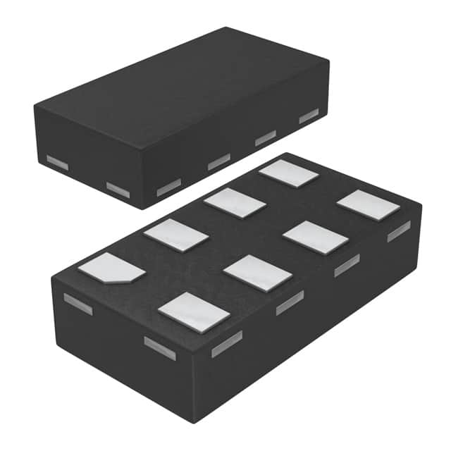
The 74AUP3G0434GFX is available in a small form factor package, such as SOT353 or XSON6, which ensures space efficiency and compatibility with various circuit designs.
Essence
The essence of this product lies in its ability to provide reliable voltage level shifting and signal buffering capabilities, ensuring proper signal integrity and compatibility between different logic levels.
Packaging/Quantity
The 74AUP3G0434GFX is typically packaged in reels or tubes, containing a specific quantity of ICs per package. The exact packaging and quantity may vary depending on the manufacturer and supplier.
Specifications
- Supply Voltage Range: 0.8V to 3.6V
- Input Voltage Range: -0.5V to VCC + 0.5V
- Output Voltage Range: 0V to VCC
- Operating Temperature Range: -40°C to +85°C
- Propagation Delay: <10ns
- Input Capacitance: <2pF
- Output Current: ±32mA
Detailed Pin Configuration
The 74AUP3G0434GFX has a total of six pins, each serving a specific function:
- VCC: Power supply input pin.
- A: Input pin for the first buffer.
- B: Input pin for the second buffer.
- C: Input pin for the third buffer.
- Y: Output pin for the buffered signal.
- GND: Ground reference pin.
Functional Features
- Schmitt-trigger inputs ensure noise immunity and hysteresis, allowing reliable operation in noisy environments.
- Triple buffering enables voltage level shifting between different logic domains.
- Low power consumption makes it suitable for battery-powered applications.
- Fast propagation delay ensures quick response time in signal processing.
Advantages and Disadvantages
Advantages
- High noise immunity ensures reliable operation in noisy environments.
- Wide operating voltage range allows compatibility with various logic levels.
- Small package size enables space-efficient circuit designs.
- Low power consumption prolongs battery life in portable devices.
Disadvantages
- Limited output current may restrict its use in high-current applications.
- Lack of built-in protection features may require additional external circuitry for certain applications.
Working Principles
The 74AUP3G0434GFX operates based on the principles of digital logic gates. It utilizes Schmitt-trigger inputs to provide noise immunity and hysteresis, ensuring stable and accurate signal processing. The triple buffering feature allows for voltage level shifting between different logic domains, enabling seamless communication between incompatible systems.
Detailed Application Field Plans
The 74AUP3G0434GFX finds applications in various fields, including but not limited to: - Microcontrollers and embedded systems - Communication systems - Industrial automation - Consumer electronics - Automotive electronics
In microcontroller-based systems, this IC can be used for level shifting between different I/O voltages. In communication systems, it aids in signal conditioning and voltage translation. In industrial automation, it facilitates interfacing between different control modules. In consumer electronics and automotive electronics, it ensures compatibility between different logic levels.
Detailed and Complete Alternative Models
- 74AUP1G04GW
- 74LVC3G34DC
- SN74LVC2G34DBVR
- NC7SZ34P5X
- TC7SZ34FU
These alternative models offer similar functionality and characteristics to the 74AUP3G0434GFX, providing options for designers based on specific requirements and availability.
Word count: 570 words
Enumere 10 preguntas y respuestas comunes relacionadas con la aplicación de 74AUP3G0434GFX en soluciones técnicas
Sure! Here are 10 common questions and answers related to the application of 74AUP3G0434GFX in technical solutions:
Q: What is the 74AUP3G0434GFX? A: The 74AUP3G0434GFX is a low-power triple buffer with Schmitt-trigger inputs, designed for voltage level translation applications.
Q: What is the operating voltage range of the 74AUP3G0434GFX? A: The operating voltage range is from 0.8V to 3.6V.
Q: Can the 74AUP3G0434GFX be used for bidirectional level shifting? A: No, the 74AUP3G0434GFX is a unidirectional buffer and cannot be used for bidirectional level shifting.
Q: What is the maximum data rate supported by the 74AUP3G0434GFX? A: The maximum data rate is typically 400 Mbps.
Q: Does the 74AUP3G0434GFX have built-in ESD protection? A: Yes, the 74AUP3G0434GFX has built-in ESD protection up to 2kV (HBM) and 200V (MM).
Q: Can the 74AUP3G0434GFX be used in automotive applications? A: Yes, the 74AUP3G0434GFX is AEC-Q100 qualified and suitable for automotive applications.
Q: What is the power supply current consumption of the 74AUP3G0434GFX? A: The power supply current consumption is typically 0.5µA in standby mode and 1.5mA in active mode.
Q: Can the 74AUP3G0434GFX be used with different supply voltages on its input and output sides? A: Yes, the 74AUP3G0434GFX supports voltage translation between different supply voltages.
Q: Does the 74AUP3G0434GFX have an open-drain output option? A: No, the 74AUP3G0434GFX only has push-pull outputs.
Q: What is the package type of the 74AUP3G0434GFX? A: The 74AUP3G0434GFX is available in a small SOT353 package.
Please note that the answers provided here are general and may vary depending on the specific datasheet and manufacturer's specifications for the 74AUP3G0434GFX.