

Consulte las especificaciones para obtener detalles del producto.
NX3DV3899GU,115
Basic Information Overview
- Category: Integrated Circuit (IC)
- Use: Digital Multiplexer/Demultiplexer Switch
- Characteristics:
- High-speed switching capability
- Low power consumption
- Compact package size
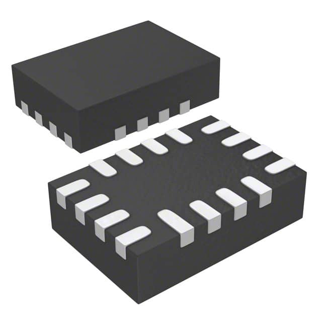
- Package: SOT1115-1 (TSSOP-16)
- Essence: This IC is designed to provide digital multiplexing and demultiplexing functionality in various electronic circuits.
- Packaging/Quantity: Available in tape and reel packaging with 2500 units per reel.
Specifications
- Supply Voltage Range: 1.65V to 4.3V
- On-state Resistance: 4Ω (typical)
- Bandwidth: Up to 400MHz
- Number of Channels: 2 channels
- Input Signal Compatibility: CMOS, TTL
- Operating Temperature Range: -40°C to +85°C
Detailed Pin Configuration
The NX3DV3899GU,115 IC has a total of 16 pins arranged as follows:
Pin 1: Channel 1 Control Input
   Pin 2: Channel 1 Data Input/Output
   Pin 3: Ground
   Pin 4: Channel 2 Data Input/Output
   Pin 5: Channel 2 Control Input
   Pin 6: VCC
   Pin 7: Channel 1 Enable Input
   Pin 8: Channel 2 Enable Input
   Pin 9: Channel 1 Output Enable Input
   Pin 10: Channel 2 Output Enable Input
   Pin 11: Channel 1 Output
   Pin 12: Channel 2 Output
   Pin 13: Channel 1 Enable Output
   Pin 14: Channel 2 Enable Output
   Pin 15: Channel 1 Output Enable Output
   Pin 16: Channel 2 Output Enable Output
Functional Features
- Digital Multiplexing: The IC allows the selection of one of two input channels to be routed to the output channel.
- Digital Demultiplexing: The IC enables the distribution of a single input signal to one of two output channels.
- High-Speed Switching: The NX3DV3899GU,115 offers fast switching times, making it suitable for high-speed data transmission applications.
- Low Power Consumption: Designed with power efficiency in mind, this IC minimizes power consumption while maintaining reliable performance.
Advantages and Disadvantages
Advantages
- Compact package size allows for space-saving integration into electronic circuits.
- Wide supply voltage range provides flexibility in various applications.
- High-speed switching capability ensures efficient data transmission.
- Low power consumption contributes to energy-efficient designs.
Disadvantages
- Limited number of channels (2 channels) may not be sufficient for complex multiplexing/demultiplexing requirements.
- Lack of built-in protection features against overvoltage or ESD events may require additional external circuitry.
Working Principles
The NX3DV3899GU,115 operates based on CMOS technology. It utilizes control inputs to select the desired input channel and enable/disable the output channels accordingly. When a specific channel is selected, the corresponding input signal is routed to the output channel. The IC's internal circuitry ensures minimal signal distortion and low power consumption during operation.
Detailed Application Field Plans
The NX3DV3899GU,115 finds applications in various electronic systems, including but not limited to: - Data communication systems - Audio/video equipment - Test and measurement instruments - Industrial automation - Consumer electronics
Detailed and Complete Alternative Models
- SN74LV4052A: Dual 4-Channel Analog Multiplexer/Demultiplexer IC by Texas Instruments.
- CD74HC4051: High-Speed CMOS Logic 8-Channel Analog Multiplexer/Demultiplexer IC by Texas Instruments.
- ADG732: Low Voltage, 32-Channel, Serially Controlled, CMOS Analog Multiplexer IC by Analog Devices.
These alternative models offer similar functionality and can be considered as alternatives to the NX3DV3899GU,115 depending on specific application requirements.
Word count: 443 words
Enumere 10 preguntas y respuestas comunes relacionadas con la aplicación de NX3DV3899GU,115 en soluciones técnicas
Sure! Here are 10 common questions and answers related to the application of NX3DV3899GU,115 in technical solutions:
1. What is the NX3DV3899GU,115? The NX3DV3899GU,115 is a high-speed, low-power, dual-supply voltage level translator IC.
2. What is the purpose of the NX3DV3899GU,115? The NX3DV3899GU,115 is designed to translate signals between different voltage domains in electronic systems.
3. What voltage levels can the NX3DV3899GU,115 support? The NX3DV3899GU,115 supports voltage translation between 1.2V and 3.6V.
4. How many channels does the NX3DV3899GU,115 have? The NX3DV3899GU,115 has 8 bidirectional channels for voltage translation.
5. What is the maximum data rate supported by the NX3DV3899GU,115? The NX3DV3899GU,115 can support data rates up to 100 Mbps.
6. Can the NX3DV3899GU,115 be used in both directions simultaneously? Yes, the NX3DV3899GU,115 supports simultaneous bidirectional translation.
7. Is the NX3DV3899GU,115 suitable for I2C and SPI interfaces? Yes, the NX3DV3899GU,115 is commonly used for voltage translation in I2C and SPI interfaces.
8. What is the power supply voltage range for the NX3DV3899GU,115? The NX3DV3899GU,115 operates with a power supply voltage range of 1.65V to 3.6V.
9. Does the NX3DV3899GU,115 require external pull-up resistors? Yes, the NX3DV3899GU,115 requires external pull-up resistors for proper operation.
10. Can the NX3DV3899GU,115 be used in battery-powered applications? Yes, the low-power characteristics of the NX3DV3899GU,115 make it suitable for battery-powered applications.
Please note that these questions and answers are general and may vary depending on specific application requirements.