

Consulte las especificaciones para obtener detalles del producto.
FGB30N6S2
Product Category
The FGB30N6S2 belongs to the category of power MOSFETs, which are electronic devices used for switching and amplifying electronic signals in various applications.
Basic Information Overview
- Use: The FGB30N6S2 is commonly used as a power switch in electronic circuits, such as motor control, power supplies, and inverters.
- Characteristics: It is known for its high voltage and current handling capabilities, low on-state resistance, and fast switching speed.
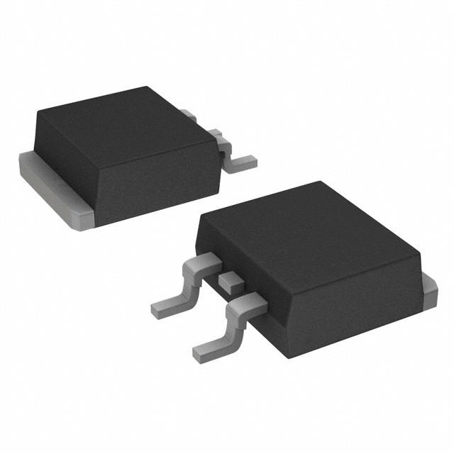
- Package: The FGB30N6S2 is typically available in a TO-220 package, which provides thermal efficiency and ease of mounting.
- Essence: This MOSFET is essential for controlling high-power loads in electronic systems.
- Packaging/Quantity: It is usually sold individually or in reels of varying quantities.
Specifications
- Voltage Rating: 600V
- Current Rating: 30A
- On-State Resistance: 0.09 ohms
- Gate Threshold Voltage: 4V
- Operating Temperature Range: -55°C to 175°C
Detailed Pin Configuration
The FGB30N6S2 typically has three pins: 1. Gate (G): Used to control the switching of the MOSFET. 2. Drain (D): Connects to the load or circuit being controlled. 3. Source (S): Connected to the ground or common reference point.
Functional Features
- High voltage and current handling capacity
- Low on-state resistance for minimal power loss
- Fast switching speed for efficient operation
- Enhanced thermal performance due to the TO-220 package
Advantages and Disadvantages
Advantages: - Suitable for high-power applications - Low power dissipation - Fast switching speed
Disadvantages: - Sensitive to static electricity - Gate drive voltage needs to be carefully controlled
Working Principles
The FGB30N6S2 operates based on the principles of field-effect transistors, where the voltage applied to the gate terminal controls the flow of current between the drain and source terminals. When the gate-source voltage reaches the threshold, the MOSFET turns on, allowing current to flow through it.
Detailed Application Field Plans
The FGB30N6S2 is widely used in various applications, including: - Motor control systems - Power supply units - Inverters for renewable energy systems - Industrial automation equipment
Detailed and Complete Alternative Models
Some alternative models to the FGB30N6S2 include: - IRF3205 - STP80NF70 - FDP8878
In conclusion, the FGB30N6S2 power MOSFET offers high-performance characteristics suitable for a wide range of high-power electronic applications, making it a popular choice among engineers and designers.
Word count: 410
Enumere 10 preguntas y respuestas comunes relacionadas con la aplicación de FGB30N6S2 en soluciones técnicas
What is FGB30N6S2?
- FGB30N6S2 is a silicon carbide (SiC) power MOSFET designed for high-frequency and high-efficiency applications.
What are the key features of FGB30N6S2?
- FGB30N6S2 features low on-resistance, fast switching speed, and high temperature operation, making it suitable for power electronics applications.
What are the typical applications of FGB30N6S2?
- FGB30N6S2 is commonly used in applications such as solar inverters, motor drives, and power supplies where high efficiency and high frequency operation are required.
What is the maximum voltage and current rating for FGB30N6S2?
- The maximum voltage rating for FGB30N6S2 is typically around 1200V, and the maximum continuous current rating is around 30A.
How does FGB30N6S2 compare to traditional silicon MOSFETs?
- FGB30N6S2 offers lower switching losses, higher temperature operation, and better performance at high frequencies compared to traditional silicon MOSFETs.
What are the thermal considerations for using FGB30N6S2?
- Proper heat sinking and thermal management are important when using FGB30N6S2 to ensure that it operates within its specified temperature limits for reliable performance.
Are there any specific gate drive requirements for FGB30N6S2?
- FGB30N6S2 may require specialized gate drive circuits to take full advantage of its fast switching speed and minimize switching losses.
Can FGB30N6S2 be used in parallel configurations for higher current applications?
- Yes, FGB30N6S2 can be used in parallel to increase the current handling capability in high-power applications.
What are the EMI considerations when using FGB30N6S2?
- FGB30N6S2's fast switching speed may generate electromagnetic interference (EMI), so proper filtering and shielding should be considered in the design.
Where can I find detailed application notes and reference designs for FGB30N6S2?
- Detailed application notes and reference designs for FGB30N6S2 can typically be found on the manufacturer's website or through their technical support resources.