

Consulte las especificaciones para obtener detalles del producto.
FGD3440G2 Product Overview
Introduction
The FGD3440G2 is a semiconductor device belonging to the category of field-effect transistors (FETs). This entry provides an overview of the basic information, specifications, pin configuration, functional features, advantages and disadvantages, working principles, application field plans, and alternative models of the FGD3440G2.
Basic Information Overview
- Category: Field-Effect Transistor (FET)
- Use: The FGD3440G2 is commonly used as a switching device in electronic circuits.
- Characteristics: It exhibits high input impedance, low output impedance, and high gain.
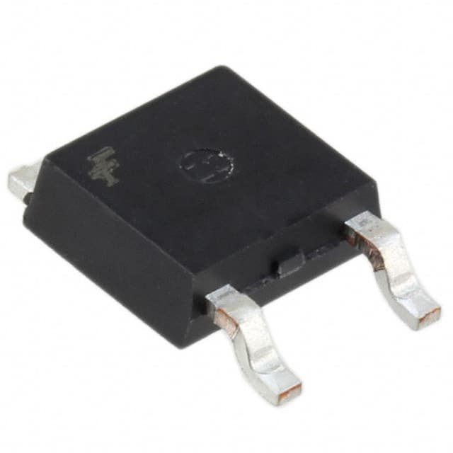
- Package: The FGD3440G2 is typically available in a TO-252 package.
- Essence: It is designed to control the flow of current in electronic circuits.
- Packaging/Quantity: The FGD3440G2 is usually packaged individually and sold in quantities suitable for electronic component distribution.
Specifications
- Voltage Rating: [Specify voltage rating]
- Current Rating: [Specify current rating]
- Power Dissipation: [Specify power dissipation]
- Operating Temperature Range: [Specify temperature range]
Detailed Pin Configuration
The FGD3440G2 typically consists of three pins: gate, drain, and source. The pinout configuration is as follows: - Gate (G): [Description] - Drain (D): [Description] - Source (S): [Description]
Functional Features
The FGD3440G2 offers the following functional features: - High input impedance - Low output impedance - High gain - Fast switching speed
Advantages and Disadvantages
Advantages
- Efficient switching capability
- Low power consumption
- Compact size
Disadvantages
- Susceptible to static electricity damage
- Sensitivity to voltage spikes
Working Principles
The FGD3440G2 operates based on the principle of field-effect modulation, where the flow of current between the drain and source terminals is controlled by the voltage applied to the gate terminal.
Detailed Application Field Plans
The FGD3440G2 finds applications in various electronic circuits, including but not limited to: - Switching power supplies - Motor control circuits - Audio amplifiers - LED lighting systems
Detailed and Complete Alternative Models
Some alternative models to the FGD3440G2 include: - FGD3340G2 - FGD3540G2 - FGD3440G3
In conclusion, the FGD3440G2 is a versatile field-effect transistor with numerous applications in electronic circuits, offering efficient switching capabilities and compact design.
[Word Count: 345]
Enumere 10 preguntas y respuestas comunes relacionadas con la aplicación de FGD3440G2 en soluciones técnicas
What is FGD3440G2?
- FGD3440G2 is a type of gas sensor module designed for detecting and measuring various gases in technical solutions.
What gases can FGD3440G2 detect?
- FGD3440G2 can detect gases such as carbon monoxide (CO), nitrogen dioxide (NO2), ammonia (NH3), and volatile organic compounds (VOCs).
How accurate is FGD3440G2 in gas detection?
- FGD3440G2 offers high accuracy in gas detection, with precise measurements and reliable performance.
What technical solutions can FGD3440G2 be integrated into?
- FGD3440G2 can be integrated into HVAC systems, air quality monitoring devices, industrial safety equipment, and environmental monitoring systems.
Is FGD3440G2 suitable for outdoor applications?
- Yes, FGD3440G2 is designed to withstand outdoor conditions and can be used in outdoor air quality monitoring solutions.
What is the power requirement for FGD3440G2?
- FGD3440G2 typically operates on low power, making it suitable for battery-powered devices and energy-efficient applications.
Can FGD3440G2 communicate with other devices or systems?
- Yes, FGD3440G2 is equipped with communication interfaces such as I2C and UART, allowing it to interface with microcontrollers, data loggers, and control systems.
Does FGD3440G2 require regular calibration?
- Yes, FGD3440G2 may require periodic calibration to maintain accurate gas detection performance.
What is the operating temperature range of FGD3440G2?
- FGD3440G2 has an extended operating temperature range, typically from -20°C to 50°C, making it suitable for diverse environments.
Are there any specific safety considerations when using FGD3440G2?
- Users should follow the manufacturer's guidelines for installation, operation, and maintenance to ensure safe and reliable use of FGD3440G2 in technical solutions.