

Consulte las especificaciones para obtener detalles del producto.
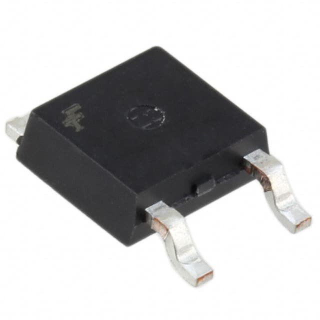
FQD10N20CTM
Introduction
The FQD10N20CTM is a power MOSFET belonging to the category of electronic components. This entry provides an overview of its basic information, specifications, pin configuration, functional features, advantages and disadvantages, working principles, application field plans, and alternative models.
Basic Information Overview
- Category: Electronic Component
- Use: Power MOSFET for electronic circuits
- Characteristics: High power handling capacity, low on-state resistance, fast switching speed
- Package: TO-252 (DPAK)
- Essence: Efficient power management in electronic devices
- Packaging/Quantity: Typically packaged in reels or tubes, quantity varies based on manufacturer
Specifications
- Voltage Rating: 200V
- Current Rating: 10A
- On-State Resistance: 0.19Ω
- Gate Threshold Voltage: 2V
- Maximum Power Dissipation: 40W
- Operating Temperature Range: -55°C to 175°C
Detailed Pin Configuration
The FQD10N20CTM typically has three pins: 1. Gate (G): Input terminal for controlling the switching of the MOSFET 2. Drain (D): Output terminal through which the current flows 3. Source (S): Terminal connected to the ground reference
Functional Features
- High voltage capability
- Low gate charge
- Fast switching speed
- Enhanced ruggedness and reliability
Advantages and Disadvantages
Advantages
- Efficient power management
- Low on-state resistance
- Fast switching speed
- High power handling capacity
Disadvantages
- Sensitivity to static electricity
- Gate driver circuitry required for proper operation
Working Principles
The FQD10N20CTM operates based on the principle of field-effect transistors, where the voltage applied to the gate terminal controls the flow of current between the drain and source terminals. When the gate-source voltage exceeds the threshold, the MOSFET turns on, allowing current to flow through it.
Detailed Application Field Plans
The FQD10N20CTM finds applications in various fields including: - Switching power supplies - Motor control - LED lighting - Battery management systems - Audio amplifiers
Detailed and Complete Alternative Models
Some alternative models to the FQD10N20CTM include: - IRF1010E - STP16NF06L - AOD4184
In conclusion, the FQD10N20CTM is a versatile power MOSFET with high power handling capacity, fast switching speed, and low on-state resistance, making it suitable for a wide range of electronic applications.
[Word Count: 386]
Enumere 10 preguntas y respuestas comunes relacionadas con la aplicación de FQD10N20CTM en soluciones técnicas
What is the maximum drain-source voltage of FQD10N20CTM?
- The maximum drain-source voltage of FQD10N20CTM is 200V.
What is the continuous drain current rating of FQD10N20CTM?
- The continuous drain current rating of FQD10N20CTM is 10A.
What is the on-resistance of FQD10N20CTM?
- The on-resistance of FQD10N20CTM is typically 0.19 ohms.
What is the gate threshold voltage of FQD10N20CTM?
- The gate threshold voltage of FQD10N20CTM is typically 2V.
Can FQD10N20CTM be used for switching applications?
- Yes, FQD10N20CTM is suitable for switching applications due to its low on-resistance and high drain-source voltage rating.
Is FQD10N20CTM suitable for motor control applications?
- Yes, FQD10N20CTM can be used in motor control applications due to its high current rating and voltage capability.
What is the typical input capacitance of FQD10N20CTM?
- The typical input capacitance of FQD10N20CTM is 800pF.
Does FQD10N20CTM require a heat sink for high-power applications?
- It is recommended to use a heat sink for high-power applications to ensure proper thermal management.
What is the operating temperature range of FQD10N20CTM?
- FQD10N20CTM has an operating temperature range of -55°C to 150°C.
Can FQD10N20CTM be used in automotive electronics applications?
- Yes, FQD10N20CTM is suitable for automotive electronics applications due to its rugged construction and high-temperature capability.