

Consulte las especificaciones para obtener detalles del producto.
J112RL1 Product Overview
Introduction
The J112RL1 is a versatile electronic component that belongs to the category of field-effect transistors (FETs). This entry provides an in-depth overview of the J112RL1, including its basic information, specifications, pin configuration, functional features, advantages and disadvantages, working principles, application field plans, and alternative models.
Basic Information Overview
- Category: Field-Effect Transistor (FET)
- Use: The J112RL1 is commonly used as a switch or amplifier in electronic circuits.
- Characteristics: It exhibits high input impedance, low output impedance, and low power consumption.
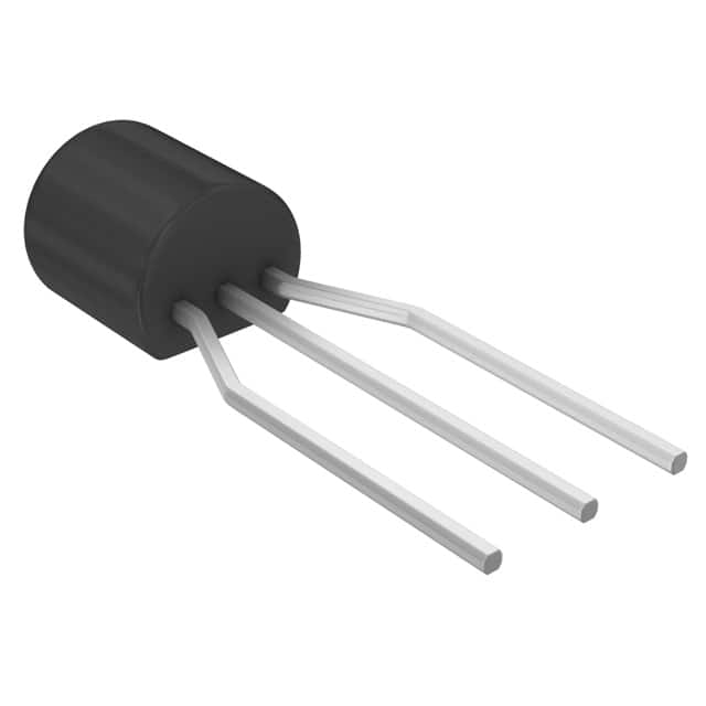
- Package: The J112RL1 is typically available in a TO-92 package.
- Essence: It is designed to provide efficient signal amplification and switching capabilities.
- Packaging/Quantity: The J112RL1 is usually sold in reels or tubes containing multiple units.
Specifications
The detailed specifications of the J112RL1 include: - Maximum Drain-Source Voltage: - Maximum Gate-Source Voltage: - Continuous Drain Current: - Total Power Dissipation: - Operating Temperature Range:
Detailed Pin Configuration
The J112RL1 features a three-pin configuration: 1. Gate (G): Controls the conductivity between the source and drain. 2. Drain (D): Connects to the positive supply in the circuit. 3. Source (S): Connects to the ground or common reference point.
Functional Features
The J112RL1 offers the following functional features: - High input impedance for minimal loading of preceding stages. - Low output impedance for driving loads with minimal signal loss. - Fast switching speed for efficient signal processing.
Advantages and Disadvantages
Advantages
- Low power consumption.
- High input impedance.
- Fast switching speed.
Disadvantages
- Susceptible to damage from electrostatic discharge (ESD).
- Limited maximum voltage and current ratings.
Working Principles
The J112RL1 operates based on the principle of field-effect modulation, where the conductivity between the source and drain is controlled by the voltage applied to the gate terminal. When the gate-source voltage is varied, the channel conductivity changes, allowing the J112RL1 to act as a switch or amplifier.
Detailed Application Field Plans
The J112RL1 finds extensive use in various applications, including: - Audio amplifiers - Signal switching circuits - Sensor interfaces - Oscillator circuits
Detailed and Complete Alternative Models
Some alternative models to the J112RL1 include: - J113RL1 - 2N7000 - BS170 - IRF510
In conclusion, the J112RL1 is a valuable FET component with versatile applications in electronic circuits, offering high input impedance, low power consumption, and fast switching speed. Its specifications, pin configuration, functional features, and alternative models make it a crucial element in modern electronics.
Word count: 411
Enumere 10 preguntas y respuestas comunes relacionadas con la aplicación de J112RL1 en soluciones técnicas
What is J112RL1?
- J112RL1 is a field-effect transistor (FET) commonly used in electronic circuits for switching and amplification.
What are the key specifications of J112RL1?
- The key specifications of J112RL1 include its maximum drain-source voltage, maximum gate-source voltage, drain current, and transconductance.
How is J112RL1 typically used in technical solutions?
- J112RL1 is often used in technical solutions for signal amplification, switching applications, and as a building block in various electronic circuits.
What are the typical applications of J112RL1 in technical solutions?
- J112RL1 is commonly used in audio amplifiers, analog switches, signal processing circuits, and voltage-controlled oscillators.
What are the advantages of using J112RL1 in technical solutions?
- Some advantages of using J112RL1 include low noise, high input impedance, and compatibility with low-voltage operation.
What are the potential drawbacks or limitations of using J112RL1?
- Drawbacks of J112RL1 may include sensitivity to electrostatic discharge (ESD), limited power handling capability, and susceptibility to thermal issues.
How can J112RL1 be integrated into a technical solution effectively?
- J112RL1 can be effectively integrated by following recommended circuit design guidelines, ensuring proper biasing, and considering thermal management.
Are there any specific considerations for driving J112RL1 in technical solutions?
- It's important to consider the gate-source voltage, input impedance, and signal levels when driving J112RL1 to ensure proper performance and reliability.
What are some common troubleshooting tips for J112RL1 in technical solutions?
- Troubleshooting tips may include checking for proper biasing, verifying connections, and testing for potential ESD damage.
Where can I find additional resources and support for using J112RL1 in technical solutions?
- Additional resources and support for J112RL1 can be found through datasheets, application notes, and manufacturer's technical support channels.