

Consulte las especificaciones para obtener detalles del producto.
MC100EP91MNR2G
Product Overview
- Category: Integrated Circuit
- Use: Signal Converter
- Characteristics: High-speed, Low-power consumption
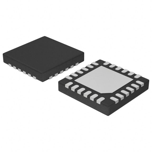
- Package: 48-pin QFN (Quad Flat No-Lead)
- Essence: Converts signals between different logic families
- Packaging/Quantity: Tape and Reel, 2500 units per reel
Specifications
- Supply Voltage: 3.3V
- Input Voltage Range: -2V to +7V
- Output Voltage Range: -2V to +7V
- Operating Temperature Range: -40°C to +85°C
- Maximum Clock Frequency: 1.6 GHz
Detailed Pin Configuration
The MC100EP91MNR2G has a total of 48 pins. The pin configuration is as follows:
- VCC
- GND
- CLKIN
- CLKSEL
- CLKOUT
- RST
- OE
- Q0
- Q1
- Q2
- Q3
- Q4
- Q5
- Q6
- Q7
- Q8
- Q9
- Q10
- Q11
- Q12
- Q13
- Q14
- Q15
- Q16
- Q17
- Q18
- Q19
- Q20
- Q21
- Q22
- Q23
- Q24
- Q25
- Q26
- Q27
- Q28
- Q29
- Q30
- Q31
- Q32
- Q33
- Q34
- Q35
- Q36
- Q37
- Q38
- Q39
- Q40
Functional Features
- Converts LVPECL (Low Voltage Positive Emitter-Coupled Logic) signals to LVCMOS (Low Voltage Complementary Metal-Oxide-Semiconductor) signals.
- Supports high-speed signal conversion up to 1.6 GHz clock frequency.
- Low-power consumption design for energy-efficient operation.
- Provides reliable signal conversion with minimal distortion.
Advantages and Disadvantages
Advantages: - High-speed signal conversion capability. - Low-power consumption for energy efficiency. - Compact package size for space-saving designs. - Reliable signal conversion with low distortion.
Disadvantages: - Limited voltage range for input and output signals. - Requires external clock source for proper operation. - Not suitable for applications requiring higher voltage levels.
Working Principles
The MC100EP91MNR2G operates based on the principles of logic level conversion. It takes in LVPECL signals as input and converts them into LVCMOS signals. The device utilizes internal circuitry to perform the necessary voltage level shifting and signal conditioning. The converted signals can then be used by downstream components that are compatible with LVCMOS logic levels.
Detailed Application Field Plans
The MC100EP91MNR2G is commonly used in various applications where signal conversion between LVPECL and LVCMOS logic families is required. Some specific application fields include:
- Telecommunications: Used in high-speed data transmission systems, such as fiber optic networks, to convert signals between different logic families.
- Networking Equipment: Integrated into routers, switches, and network interface cards to enable compatibility between different logic standards.
- Test and Measurement Instruments: Employed in oscilloscopes, logic analyzers, and other test equipment to facilitate signal conversion during signal analysis and testing processes.
- Industrial Automation: Utilized in control systems and PLCs (Programmable Logic Controllers) to interface between different logic families used in industrial machinery and equipment.
Detailed and Complete Alternative Models
- MC100EP91MNG
- MC100EP91MN
- MC100EP91MNR2
- MC100EP91MNR2G-ND
- MC100EP91MNR2GOSCT-ND
These alternative models offer similar functionality and can be considered as substitutes for the MC100EP91MNR2G based on specific requirements and availability.
Enumere 10 preguntas y respuestas comunes relacionadas con la aplicación de MC100EP91MNR2G en soluciones técnicas
Sure! Here are 10 common questions and answers related to the application of MC100EP91MNR2G in technical solutions:
Question: What is MC100EP91MNR2G?
- Answer: MC100EP91MNR2G is a high-speed, low-skew 1:9 differential ECL/PECL fanout buffer.Question: What is the operating voltage range for MC100EP91MNR2G?
- Answer: The operating voltage range for MC100EP91MNR2G is between -4.2V and -5.7V.Question: What is the maximum operating frequency supported by MC100EP91MNR2G?
- Answer: MC100EP91MNR2G supports a maximum operating frequency of 3.8 GHz.Question: Can MC100EP91MNR2G be used as a clock distribution buffer?
- Answer: Yes, MC100EP91MNR2G can be used as a clock distribution buffer due to its low skew characteristics.Question: What is the output type of MC100EP91MNR2G?
- Answer: MC100EP91MNR2G has differential outputs that can be configured as either ECL or PECL.Question: Is MC100EP91MNR2G suitable for high-speed data transmission applications?
- Answer: Yes, MC100EP91MNR2G is designed for high-speed applications such as data transmission and clock distribution.Question: Does MC100EP91MNR2G have any built-in input termination resistors?
- Answer: No, MC100EP91MNR2G does not have built-in input termination resistors. External termination may be required depending on the application.Question: What is the typical output skew of MC100EP91MNR2G?
- Answer: The typical output skew of MC100EP91MNR2G is less than 50 ps.Question: Can MC100EP91MNR2G be used in both single-ended and differential input applications?
- Answer: No, MC100EP91MNR2G is specifically designed for differential input applications.Question: Are there any specific layout considerations for using MC100EP91MNR2G?
- Answer: Yes, it is recommended to follow the layout guidelines provided in the datasheet to ensure optimal performance and minimize signal integrity issues.
Please note that these answers are general and may vary depending on the specific requirements and implementation of MC100EP91MNR2G in a technical solution.