

Consulte las especificaciones para obtener detalles del producto.
NC7WV07P6X
Product Overview
- Category: Integrated Circuit
- Use: Logic Gate
- Characteristics: Low Voltage, High-Speed, Dual Buffer/Driver
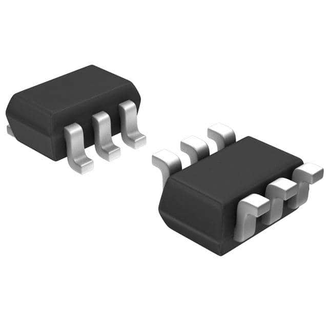
- Package: X2SON-6
- Essence: Compact and efficient logic gate solution
- Packaging/Quantity: Tape and Reel, 3000 units per reel
Specifications
- Supply Voltage: 1.65V to 5.5V
- Logic Family: CMOS
- Number of Inputs: 2
- Number of Outputs: 2
- Propagation Delay: 2.5ns (typical)
- Operating Temperature Range: -40°C to +85°C
Detailed Pin Configuration
The NC7WV07P6X has a total of six pins arranged as follows:
____
   VCC |    | GND
   IN1 |    | OUT1
   IN2 |    | OUT2
        ----
- VCC: Power supply pin (+)
- GND: Ground pin (-)
- IN1: Input 1 pin
- OUT1: Output 1 pin
- IN2: Input 2 pin
- OUT2: Output 2 pin
Functional Features
- Dual buffer/driver with independent inputs and outputs
- Wide operating voltage range allows compatibility with various systems
- High-speed operation for quick signal processing
- Low power consumption for energy-efficient applications
- Compact X2SON-6 package enables space-saving designs
Advantages and Disadvantages
Advantages
- Versatile logic gate suitable for a wide range of applications
- Low voltage operation extends battery life in portable devices
- Fast propagation delay ensures rapid signal transmission
- Small package size enables compact circuit designs
Disadvantages
- Limited number of inputs and outputs may restrict complex circuit configurations
- Operating temperature range may not be suitable for extreme environments
Working Principles
The NC7WV07P6X is a CMOS logic gate that functions as a dual buffer/driver. It operates by receiving input signals at the IN1 and IN2 pins, and then amplifying and driving those signals to the corresponding OUT1 and OUT2 pins. The device operates within a specified voltage range and utilizes CMOS technology to achieve low power consumption and high-speed performance.
Detailed Application Field Plans
The NC7WV07P6X finds applications in various fields, including:
- Consumer Electronics: Used in smartphones, tablets, and wearable devices for signal buffering and level shifting.
- Automotive: Employed in automotive electronics for voltage level translation and signal amplification.
- Industrial Automation: Utilized in control systems and sensors for logic signal conditioning.
- Communication Systems: Integrated into networking equipment and data transmission devices for signal processing and amplification.
Detailed and Complete Alternative Models
- SN74LVC07A: Similar dual buffer/driver with 5V tolerant inputs and outputs.
- MC74LVX07: Dual buffer/driver with Schmitt-trigger inputs for noise immunity.
- CD40107B: Dual J-K flip-flop with complementary buffered outputs.
These alternative models offer similar functionality and can be considered as substitutes for the NC7WV07P6X depending on specific requirements.
Word count: 410 words
Enumere 10 preguntas y respuestas comunes relacionadas con la aplicación de NC7WV07P6X en soluciones técnicas
Sure! Here are 10 common questions and answers related to the application of NC7WV07P6X in technical solutions:
Question: What is NC7WV07P6X?
Answer: NC7WV07P6X is a specific type of integrated circuit (IC) known as a buffer/driver, commonly used in digital logic applications.Question: What is the purpose of using NC7WV07P6X in technical solutions?
Answer: The NC7WV07P6X is used to provide voltage level shifting and signal buffering capabilities, ensuring proper communication between different components or subsystems in a circuit.Question: What voltage levels can NC7WV07P6X handle?
Answer: NC7WV07P6X can handle voltage levels ranging from 1.65V to 5.5V, making it compatible with various digital logic families.Question: Can NC7WV07P6X be used for bidirectional communication?
Answer: Yes, NC7WV07P6X supports bidirectional communication, allowing signals to be transmitted in both directions.Question: How many channels does NC7WV07P6X have?
Answer: NC7WV07P6X has six independent channels, each capable of handling a separate signal.Question: What is the maximum data rate supported by NC7WV07P6X?
Answer: NC7WV07P6X can support data rates up to 100 Mbps, making it suitable for high-speed digital communication.Question: Is NC7WV07P6X suitable for battery-powered applications?
Answer: Yes, NC7WV07P6X is designed to operate at low power, making it suitable for battery-powered applications where power consumption is a concern.Question: Can NC7WV07P6X tolerate overvoltage or ESD events?
Answer: NC7WV07P6X has built-in protection features to withstand overvoltage and electrostatic discharge (ESD) events, ensuring the reliability of the circuit.Question: What package options are available for NC7WV07P6X?
Answer: NC7WV07P6X is available in various package options, including SOT-23, SC-70, and X2SON, providing flexibility for different PCB layouts.Question: Are there any application notes or reference designs available for NC7WV07P6X?
Answer: Yes, the manufacturer of NC7WV07P6X provides application notes and reference designs that can help engineers understand and implement the IC effectively in their technical solutions.
Please note that the answers provided here are general and may vary depending on specific requirements and use cases. It's always recommended to refer to the datasheet and documentation provided by the manufacturer for detailed information.