

Consulte las especificaciones para obtener detalles del producto.
STW70N60DM2
Introduction
The STW70N60DM2 is a power MOSFET belonging to the category of semiconductor devices. It is widely used in various electronic applications due to its unique characteristics and performance.
Basic Information Overview
- Category: Semiconductor Device
- Use: Power switching applications
- Characteristics: High voltage capability, low on-resistance, fast switching speed
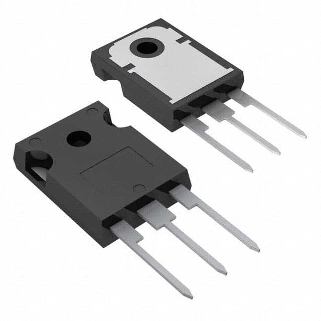
- Package: TO-247
- Essence: Efficient power management
- Packaging/Quantity: Typically sold in reels of 1000 units
Specifications
- Voltage Rating: 600V
- Current Rating: 70A
- On-Resistance: 0.036Ω
- Gate Charge: 45nC
- Operating Temperature Range: -55°C to 150°C
Detailed Pin Configuration
The STW70N60DM2 features a standard TO-247 pin configuration with three pins: gate (G), drain (D), and source (S).
Functional Features
- High voltage capability for power applications
- Low on-resistance for reduced power dissipation
- Fast switching speed for improved efficiency
Advantages and Disadvantages
Advantages: - High voltage capability enables use in diverse applications - Low on-resistance leads to reduced power losses - Fast switching speed enhances overall efficiency
Disadvantages: - Higher cost compared to lower-rated MOSFETs - Requires careful handling due to sensitivity to static electricity
Working Principles
The STW70N60DM2 operates based on the principles of field-effect transistors, utilizing the control of an electric field to modulate the conductivity of the device. When a suitable voltage is applied to the gate terminal, it allows or restricts the flow of current between the drain and source terminals.
Detailed Application Field Plans
The STW70N60DM2 finds extensive use in various power electronics applications, including: - Switch-mode power supplies - Motor control systems - Inverters and converters - Industrial automation equipment
Detailed and Complete Alternative Models
- STW80N60DM2: Similar specifications with higher current rating
- STW60N60DM2: Similar specifications with lower current rating
- STW90N60DM2: Similar specifications with higher voltage rating
In conclusion, the STW70N60DM2 is a versatile power MOSFET with high voltage capability, low on-resistance, and fast switching speed, making it an ideal choice for various power switching applications.
[Word Count: 309]
Enumere 10 preguntas y respuestas comunes relacionadas con la aplicación de STW70N60DM2 en soluciones técnicas
What is the maximum drain-source voltage of STW70N60DM2?
- The maximum drain-source voltage of STW70N60DM2 is 600V.
What is the continuous drain current rating of STW70N60DM2?
- The continuous drain current rating of STW70N60DM2 is 70A.
What is the on-state resistance (RDS(on)) of STW70N60DM2?
- The on-state resistance (RDS(on)) of STW70N60DM2 is typically 0.045 ohms.
What is the gate threshold voltage of STW70N60DM2?
- The gate threshold voltage of STW70N60DM2 is typically 3V.
What are the typical applications for STW70N60DM2?
- STW70N60DM2 is commonly used in applications such as motor control, power supplies, and inverters.
What is the operating temperature range of STW70N60DM2?
- The operating temperature range of STW70N60DM2 is typically -55°C to 150°C.
Does STW70N60DM2 require a heat sink for operation?
- Yes, STW70N60DM2 may require a heat sink depending on the application and power dissipation requirements.
Is STW70N60DM2 suitable for high-frequency switching applications?
- Yes, STW70N60DM2 is suitable for high-frequency switching due to its low RDS(on) and fast switching characteristics.
What are the recommended gate driver specifications for STW70N60DM2?
- It is recommended to use a gate driver capable of providing sufficient gate-source voltage and current for optimal performance of STW70N60DM2.
Are there any specific layout considerations when using STW70N60DM2 in a circuit?
- Proper PCB layout, including minimizing parasitic inductance and ensuring proper thermal management, is important for maximizing the performance and reliability of STW70N60DM2.