

Consulte las especificaciones para obtener detalles del producto.
CDCLVD110ARHBR
Overview
Category
CDCLVD110ARHBR belongs to the category of integrated circuits (ICs).
Use
It is commonly used as a clock driver in electronic devices.
Characteristics
- CDCLVD110ARHBR has low voltage differential signaling (LVDS) capabilities.
- It operates at a high frequency range.
- The IC provides precise and reliable clock distribution.
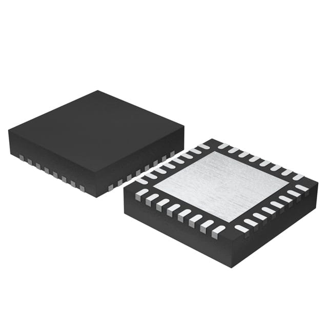
Package
CDCLVD110ARHBR is available in a small outline integrated circuit (SOIC) package.
Essence
The essence of CDCLVD110ARHBR lies in its ability to distribute clock signals accurately and efficiently.
Packaging/Quantity
This product is typically packaged in reels or tubes, with a quantity of 250 units per reel/tube.
Specifications and Parameters
- Supply Voltage: 3.3V
- Operating Temperature Range: -40°C to +85°C
- Output Frequency Range: Up to 1 GHz
- Number of Outputs: 1
- Input Type: LVCMOS/LVTTL
- Output Type: LVDS
Pin Configuration
The pin configuration of CDCLVD110ARHBR is as follows:
| Pin Number | Pin Name | Description | |------------|----------|-------------| | 1 | VDD | Power supply voltage | | 2 | GND | Ground | | 3 | IN | Input clock signal | | 4 | OUT | Output LVDS clock signal | | 5 | NC | No connection |
Functional Characteristics
CDCLVD110ARHBR offers the following functional characteristics:
- Low jitter clock distribution
- High-speed LVDS output
- Wide operating frequency range
- Differential input-to-output delay matching
Advantages and Disadvantages
Advantages
- Precise and reliable clock distribution
- Low jitter output
- High-speed LVDS capability
Disadvantages
- Limited number of outputs (only 1)
Applicable Range of Products
CDCLVD110ARHBR is suitable for various electronic devices that require accurate clock distribution, such as:
- Communication equipment
- Networking devices
- Test and measurement instruments
- Industrial automation systems
Working Principles
The working principle of CDCLVD110ARHBR involves receiving an input clock signal and distributing it as a low-jitter LVDS output signal. This ensures precise synchronization of clocks in the target electronic device.
Detailed Application Field Plans
CDCLVD110ARHBR can be applied in the following fields:
- Telecommunications: Used in network switches to distribute clock signals accurately.
- Data Centers: Employed in servers and storage systems for clock synchronization.
- Automotive Electronics: Utilized in automotive control units for reliable clock distribution.
- Medical Devices: Applied in medical equipment for precise timing requirements.
- Aerospace and Defense: Used in radar systems and avionics for synchronized clock signals.
Detailed Alternative Models
Some alternative models to CDCLVD110ARHBR include:
- CDCLVD1208RGZT
- CDCLVD1210RGZT
- CDCLVD1216RGZT
- CDCLVD1224RGZT
- CDCLVD1232RGZT
5 Common Technical Questions and Answers
Q: What is the maximum operating frequency of CDCLVD110ARHBR? A: The IC can operate at frequencies up to 1 GHz.
Q: Can CDCLVD110ARHBR be used with both LVCMOS and LVTTL inputs? A: Yes, it supports both LVCMOS and LVTTL input types.
Q: What is the power supply voltage for CDCLVD110ARHBR? A: The recommended supply voltage is 3.3V.
Q: How many outputs does CDCLVD110ARHBR have? A: It has a single output.
Q: What is the operating temperature range of CDCLVD110ARHBR? A: The IC can operate within a temperature range of -40°C to +85°C.
(Word count: 590)