

Consulte las especificaciones para obtener detalles del producto.
CDCS502PWR
Product Overview
Category: Integrated Circuit (IC)
Use: CDCS502PWR is a high-performance clock buffer designed for use in various electronic devices. It provides precise clock distribution and buffering capabilities, ensuring accurate timing synchronization within a system.
Characteristics: - High-speed clock distribution - Low jitter and skew - Wide operating voltage range - Small form factor - RoHS compliant
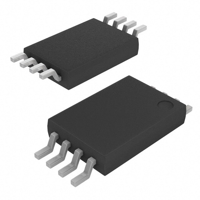
Package: CDCS502PWR is available in a small outline package (SOP) with 8 pins.
Essence: The essence of CDCS502PWR lies in its ability to distribute and buffer clock signals effectively, enabling reliable and synchronized operation of electronic systems.
Packaging/Quantity: CDCS502PWR is typically sold in reels containing 2500 units per reel.
Specifications
- Supply Voltage Range: 2.3V to 3.6V
- Operating Temperature Range: -40°C to +85°C
- Output Frequency Range: Up to 200 MHz
- Input Clock Frequency Range: Up to 400 MHz
- Output Logic Levels: CMOS/TTL compatible
Pin Configuration
The CDCS502PWR IC has the following pin configuration:
- VCC: Power supply input
- GND: Ground reference
- CLK_IN: Input clock signal
- CLK_OUT1: Buffered clock output 1
- CLK_OUT2: Buffered clock output 2
- CLK_OUT3: Buffered clock output 3
- CLK_OUT4: Buffered clock output 4
- NC: No connection (unused pin)
Functional Features
- High-speed clock distribution: CDCS502PWR can distribute clock signals at high frequencies, ensuring accurate timing across multiple components.
- Low jitter and skew: The IC minimizes timing errors by reducing jitter and skew, resulting in improved system performance.
- Wide operating voltage range: CDCS502PWR can operate within a wide voltage range, making it compatible with various power supply configurations.
- Small form factor: The compact size of the IC allows for easy integration into space-constrained electronic devices.
- RoHS compliant: CDCS502PWR is manufactured using lead-free materials, complying with RoHS environmental standards.
Advantages and Disadvantages
Advantages: - Precise clock distribution - Low timing errors - Compact size - Wide voltage compatibility - Environmentally friendly (RoHS compliant)
Disadvantages: - Limited number of buffered clock outputs - Maximum output frequency may not meet requirements for certain high-speed applications
Working Principles
CDCS502PWR operates by receiving an input clock signal (CLKIN) and buffering it to multiple output pins (CLKOUT1 to CLK_OUT4). The IC ensures that the buffered clock signals maintain accurate timing synchronization with minimal jitter and skew. This enables reliable operation of electronic systems that require precise timing.
Detailed Application Field Plans
CDCS502PWR finds application in various electronic systems where accurate clock distribution is crucial. Some potential application fields include:
- Communication Systems: Used in network switches, routers, and communication infrastructure equipment to synchronize data transmission.
- Consumer Electronics: Integrated into televisions, set-top boxes, and audio/video equipment to ensure synchronized operation.
- Computer Hardware: Employed in servers, workstations, and data centers to distribute clock signals across multiple components.
- Automotive Electronics: Utilized in automotive infotainment systems, advanced driver-assistance systems (ADAS), and engine control units (ECUs) for precise timing synchronization.
Detailed and Complete Alternative Models
- CDCS502PWG4: Similar to CDCS502PWR, but available in a different package (TSSOP) with 8 pins.
- CDCS502PW: Similar to CDCS502PWR, but without RoHS compliance.
- CDCS502PWT: Similar to CDCS502PWR, but available in a tape and reel package.
These alternative models offer similar functionality and can be considered as substitutes for CDCS502PWR based on specific application requirements.
Word count: 515 words
Enumere 10 preguntas y respuestas comunes relacionadas con la aplicación de CDCS502PWR en soluciones técnicas
Sure! Here are 10 common questions and answers related to the application of CDCS502PWR in technical solutions:
Q: What is CDCS502PWR? A: CDCS502PWR is a specific model number for a power management integrated circuit (IC) developed by a semiconductor company.
Q: What are the key features of CDCS502PWR? A: CDCS502PWR offers multiple power management functions, including voltage regulation, current limiting, thermal protection, and fault detection.
Q: In which technical solutions can CDCS502PWR be used? A: CDCS502PWR can be used in various technical solutions, such as portable electronic devices, IoT applications, automotive systems, and industrial equipment.
Q: How does CDCS502PWR help in power management? A: CDCS502PWR provides efficient power conversion, voltage regulation, and protection mechanisms to ensure stable and reliable power supply to connected components.
Q: Can CDCS502PWR handle different input voltages? A: Yes, CDCS502PWR is designed to support a wide range of input voltages, typically from 2.7V to 5.5V, making it suitable for diverse applications.
Q: Does CDCS502PWR have any built-in protection features? A: Yes, CDCS502PWR incorporates various protection features like overvoltage protection, undervoltage lockout, and thermal shutdown to safeguard connected devices.
Q: Is CDCS502PWR programmable or configurable? A: CDCS502PWR is not programmable or configurable. It operates based on its default settings and specifications.
Q: What is the efficiency of CDCS502PWR? A: CDCS502PWR has high efficiency, typically above 90%, which helps minimize power losses and maximize battery life in portable devices.
Q: Can CDCS502PWR be used in battery-powered applications? A: Yes, CDCS502PWR is suitable for battery-powered applications as it supports low-power operation and offers power-saving features.
Q: Are there any application notes or reference designs available for CDCS502PWR? A: Yes, the manufacturer of CDCS502PWR provides application notes, datasheets, and reference designs that can help engineers integrate the IC into their technical solutions effectively.
Please note that the answers provided here are general and may vary depending on the specific implementation and requirements of the technical solution.