

Consulte las especificaciones para obtener detalles del producto.
DAC101C081QISD/NOPB
Product Overview
Category: Digital-to-Analog Converter (DAC)
Use: The DAC101C081QISD/NOPB is a high-performance, low-power, 10-bit digital-to-analog converter designed for various applications that require precise analog output generation. It converts digital input signals into corresponding analog voltage levels.
Characteristics: - High precision and accuracy - Low power consumption - Small package size - Wide operating temperature range - Excellent linearity and monotonicity - Fast settling time
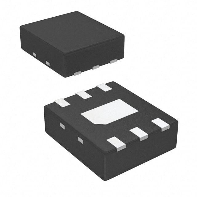
Package: The DAC101C081QISD/NOPB comes in a small outline integrated circuit (SOIC) package, which ensures easy integration into different electronic systems.
Essence: This DAC provides a reliable and efficient solution for generating accurate analog signals from digital inputs, making it suitable for a wide range of applications.
Packaging/Quantity: The DAC101C081QISD/NOPB is typically available in reels or tubes, with a quantity of 2500 units per reel/tube.
Specifications
- Resolution: 10 bits
- Supply Voltage: 2.7V to 5.5V
- Output Voltage Range: 0V to Vref
- Operating Temperature Range: -40°C to +125°C
- Total Unadjusted Error: ±1 LSB (maximum)
- Power Consumption: 0.6mW (typical)
- Settling Time: 4µs (typical)
Pin Configuration
The DAC101C081QISD/NOPB has the following pin configuration:
┌───┬───┐
   │ 1 │ 8 │
   │   │   │
   │   │   │
   │   │   │
   │   │   │
   │   │   │
   │   │   │
   │ 2 │ 7 │
   └───┴───┘
Pin 1: Vref (Reference Voltage Input)
Pin 2: Vout (Analog Output)
Pin 7: GND (Ground)
Pin 8: VDD (Supply Voltage)
Functional Features
- High-resolution digital-to-analog conversion
- Low power consumption for energy-efficient operation
- Fast settling time ensures quick response to input changes
- Excellent linearity and monotonicity for accurate analog output
- Wide operating temperature range allows for versatile usage in various environments
Advantages and Disadvantages
Advantages: - High precision and accuracy - Low power consumption - Small package size for easy integration - Wide operating temperature range - Fast settling time for quick response
Disadvantages: - Limited resolution compared to higher-bit DACs - May require external components for certain applications
Working Principles
The DAC101C081QISD/NOPB operates on the principle of converting digital input signals into corresponding analog voltage levels. It utilizes an internal digital-to-analog conversion algorithm to accurately generate the desired analog output. The reference voltage (Vref) determines the maximum output voltage, while the digital input controls the output voltage level.
Detailed Application Field Plans
The DAC101C081QISD/NOPB finds applications in various fields, including but not limited to: - Industrial automation - Test and measurement equipment - Audio systems - Communication devices - Medical instruments - Automotive electronics
Alternative Models
For alternative options with similar functionality, consider the following models: - DAC102S085CIMM/NOPB - DAC121S101CIMK/NOPB - DAC0830LCN/NOPB - DAC8562SDGSR
These models offer different resolutions, package types, or additional features to suit specific application requirements.
In conclusion, the DAC101C081QISD/NOPB is a high-performance digital-to-analog converter that provides accurate analog output generation with low power consumption. Its small package size and wide operating temperature range make it suitable for various applications in different industries.
Enumere 10 preguntas y respuestas comunes relacionadas con la aplicación de DAC101C081QISD/NOPB en soluciones técnicas
What is the input voltage range of DAC101C081QISD/NOPB?
- The input voltage range of DAC101C081QISD/NOPB is 2.7V to 5.5V.What is the resolution of DAC101C081QISD/NOPB?
- DAC101C081QISD/NOPB has a resolution of 10 bits.Can DAC101C081QISD/NOPB be used in industrial control applications?
- Yes, DAC101C081QISD/NOPB is suitable for industrial control applications.What is the output voltage range of DAC101C081QISD/NOPB?
- The output voltage range of DAC101C081QISD/NOPB is 0V to Vref.Is DAC101C081QISD/NOPB compatible with SPI interface?
- Yes, DAC101C081QISD/NOPB supports SPI interface.Can DAC101C081QISD/NOPB be used in battery-powered devices?
- Yes, DAC101C081QISD/NOPB is suitable for battery-powered devices due to its low power consumption.What is the typical settling time of DAC101C081QISD/NOPB?
- The typical settling time of DAC101C081QISD/NOPB is 6µs.Does DAC101C081QISD/NOPB have internal reference voltage?
- No, DAC101C081QISD/NOPB requires an external reference voltage.Is DAC101C081QISD/NOPB suitable for audio applications?
- Yes, DAC101C081QISD/NOPB can be used in audio applications.What is the package type of DAC101C081QISD/NOPB?
- DAC101C081QISD/NOPB comes in a small 6-pin SOT-23 package.