

Consulte las especificaciones para obtener detalles del producto.
DAC8551IDGKT
Product Overview
Category: Digital-to-Analog Converter (DAC)
Use: The DAC8551IDGKT is a high-precision, low-power, 16-bit digital-to-analog converter. It is designed to convert digital signals into analog voltages with exceptional accuracy and linearity.
Characteristics: - High precision: The DAC8551IDGKT offers 16-bit resolution, providing precise control over the output voltage. - Low power consumption: This DAC operates at a low power supply voltage of 2.7V to 5.5V, making it suitable for battery-powered applications. - Small package: The DAC8551IDGKT comes in a compact MSOP-10 package, allowing for space-efficient integration into various electronic systems. - SPI interface: It utilizes a Serial Peripheral Interface (SPI) for easy communication with microcontrollers or other digital devices. - Rail-to-rail output: The DAC provides rail-to-rail output voltage swing, enabling it to generate the full-scale output voltage across the entire power supply range.
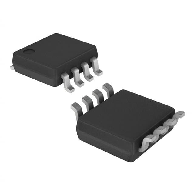
Package and Quantity: The DAC8551IDGKT is available in a tape-and-reel packaging format, with 2500 units per reel.
Specifications
- Resolution: 16 bits
- Supply Voltage Range: 2.7V to 5.5V
- Output Voltage Range: 0V to Vref
- Operating Temperature Range: -40°C to +105°C
- DNL (Differential Non-Linearity): ±0.5 LSB (max)
- INL (Integral Non-Linearity): ±1 LSB (max)
- Power Consumption: 0.4mW (typical)
Pin Configuration
The DAC8551IDGKT features the following pin configuration:
```
| | | DAC8551IDGKT | |_______________________________________| | | | VDD DIN SCLK CS GND VOUT | |_______________________________________| ```
- VDD: Power supply voltage
- DIN: Serial data input
- SCLK: Serial clock input
- CS: Chip select input
- GND: Ground reference
- VOUT: Analog output voltage
Functional Features
- High-resolution conversion: The DAC8551IDGKT offers 16-bit resolution, allowing for precise control of analog output voltages.
- Low power consumption: With a low power supply voltage range and efficient design, this DAC minimizes power consumption in various applications.
- Easy integration: The SPI interface simplifies communication with microcontrollers or other digital devices, enabling seamless integration into electronic systems.
- Rail-to-rail output swing: The DAC provides a wide output voltage range, ensuring accurate representation of the full-scale output voltage.
Advantages and Disadvantages
Advantages: - High precision and linearity - Low power consumption - Compact package size - Wide operating temperature range - Easy integration with microcontrollers
Disadvantages: - Limited output voltage range compared to some other DACs - Requires an external voltage reference for accurate conversions
Working Principles
The DAC8551IDGKT operates by converting digital input signals into corresponding analog output voltages. It utilizes a 16-bit digital word to determine the output voltage level. The input digital data is received through the DIN pin and synchronized with the serial clock (SCLK) signal. The chip select (CS) pin enables the DAC for data transfer. Once the digital data is received, the DAC performs a conversion and generates the corresponding analog voltage at the VOUT pin.
Detailed Application Field Plans
The DAC8551IDGKT finds applications in various fields, including:
- Industrial Automation: It can be used for precise control of analog signals in industrial automation systems, such as motor control, process control, and instrumentation.
- Audio Systems: The DAC is suitable for audio applications, including digital audio players, audio mixers, and professional audio equipment, where high-resolution conversion is required.
- Test and Measurement: It can be utilized in test and measurement equipment, providing accurate analog voltage generation for calibration, signal generation, and waveform synthesis.
- Communication Systems: The DAC finds application in communication systems, enabling the generation of analog signals for modulation, demodulation, and signal conditioning.
Detailed and Complete Alternative Models
- DAC8550IDGKT: Similar to the DAC8551IDGKT, but with a single buffered output instead of rail-to-rail output swing.
- DAC8552IDGKT: Dual-channel version of the DAC8551IDGKT, offering two independent 16-bit DACs in a single package.
- DAC8562IDGKT: Higher-resolution DAC with 18-bit resolution, suitable for applications requiring even greater
Enumere 10 preguntas y respuestas comunes relacionadas con la aplicación de DAC8551IDGKT en soluciones técnicas
Sure! Here are 10 common questions and answers related to the application of DAC8551IDGKT:
Q1: What is DAC8551IDGKT? A1: DAC8551IDGKT is a digital-to-analog converter (DAC) IC manufactured by Texas Instruments. It converts digital signals into analog voltages.
Q2: What is the operating voltage range of DAC8551IDGKT? A2: The operating voltage range of DAC8551IDGKT is typically between 2.7V and 5.5V.
Q3: How many channels does DAC8551IDGKT have? A3: DAC8551IDGKT has a single channel, meaning it can convert one digital signal into an analog voltage at a time.
Q4: What is the resolution of DAC8551IDGKT? A4: DAC8551IDGKT has a resolution of 16 bits, which means it can provide 65,536 different output voltage levels.
Q5: Can DAC8551IDGKT be used for both voltage and current output? A5: Yes, DAC8551IDGKT can be configured for both voltage and current output modes, depending on the application requirements.
Q6: What is the maximum output voltage range of DAC8551IDGKT? A6: The maximum output voltage range of DAC8551IDGKT is determined by the reference voltage provided to the device. It can be set up to Vref, where Vref is the reference voltage.
Q7: Does DAC8551IDGKT support SPI communication? A7: Yes, DAC8551IDGKT supports Serial Peripheral Interface (SPI) communication protocol, making it easy to interface with microcontrollers and other digital devices.
Q8: Can DAC8551IDGKT operate in both single-ended and differential output modes? A8: Yes, DAC8551IDGKT can be configured for both single-ended and differential output modes, depending on the application requirements.
Q9: What is the typical settling time of DAC8551IDGKT? A9: The typical settling time of DAC8551IDGKT is around 10 microseconds, which means it takes approximately 10 microseconds for the output voltage to stabilize after a change in the digital input.
Q10: Can multiple DAC8551IDGKT devices be cascaded together? A10: Yes, multiple DAC8551IDGKT devices can be cascaded together using the SPI interface, allowing for the simultaneous control of multiple channels or the creation of higher-resolution outputs.
Please note that these answers are general and may vary depending on specific datasheet specifications and application requirements.