

Consulte las especificaciones para obtener detalles del producto.
SN55451BJG
Product Overview
Category
SN55451BJG belongs to the category of integrated circuits (ICs).
Use
This product is commonly used in electronic devices for signal conditioning and amplification.
Characteristics
- Signal conditioning and amplification capabilities
- High precision and accuracy
- Low power consumption
- Compact size
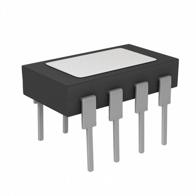
Package
SN55451BJG is available in a small outline package (SOP) or dual in-line package (DIP).
Essence
The essence of SN55451BJG lies in its ability to enhance and condition electrical signals, making it suitable for various applications.
Packaging/Quantity
SN55451BJG is typically packaged in reels or tubes, with quantities varying depending on customer requirements.
Specifications
- Supply Voltage: 3.3V - 5V
- Operating Temperature Range: -40°C to +85°C
- Input Voltage Range: ±10V
- Gain Bandwidth Product: 1 MHz
- Output Current: 20 mA
- Input Bias Current: 100 nA
- Package Type: SOP-8/DIP-8
Detailed Pin Configuration
- VCC: Power supply input
- IN+: Non-inverting input
- IN-: Inverting input
- OUT: Amplified output
- GND: Ground connection
- NC: No connection
- NC: No connection
- VEE: Negative power supply input
Functional Features
- High gain amplification
- Differential input configuration
- Wide input voltage range
- Low distortion and noise
- Rail-to-rail output swing
Advantages
- Versatile and adaptable to various applications
- Low power consumption prolongs battery life
- Small form factor allows for space-saving designs
- Excellent signal conditioning capabilities
- Reliable and durable performance
Disadvantages
- Limited output current may not be suitable for high-power applications
- Requires external power supply for operation
- Sensitivity to electromagnetic interference (EMI)
Working Principles
SN55451BJG operates based on the principles of differential amplification. It amplifies the voltage difference between the non-inverting and inverting inputs, providing an amplified output signal.
Detailed Application Field Plans
SN55451BJG finds applications in various fields, including:
- Audio equipment: Amplifying audio signals for speakers and headphones.
- Sensor interfaces: Conditioning and amplifying signals from sensors such as temperature, pressure, and light sensors.
- Communication systems: Signal conditioning in wireless communication devices.
- Industrial automation: Signal processing in control systems and data acquisition.
Detailed and Complete Alternative Models
- LM358: Dual operational amplifier with similar characteristics.
- TL071: Low-noise JFET-input operational amplifier.
- AD822: Precision instrumentation amplifier for sensor signal conditioning.
Note: This is not an exhaustive list, and there are several alternative models available in the market.
Word count: 439 words
Enumere 10 preguntas y respuestas comunes relacionadas con la aplicación de SN55451BJG en soluciones técnicas
Sure! Here are 10 common questions and answers related to the application of SN55451BJG in technical solutions:
Q: What is SN55451BJG? A: SN55451BJG is a specific integrated circuit (IC) chip used in various technical applications.
Q: What is the purpose of SN55451BJG? A: SN55451BJG is commonly used as a voltage comparator or operational amplifier in electronic circuits.
Q: What is the operating voltage range for SN55451BJG? A: The operating voltage range for SN55451BJG typically falls between 2V and 36V.
Q: What is the maximum output current of SN55451BJG? A: The maximum output current of SN55451BJG is usually around 20mA.
Q: Can SN55451BJG be used in low-power applications? A: Yes, SN55451BJG is suitable for low-power applications due to its low quiescent current consumption.
Q: Is SN55451BJG compatible with both single and dual power supply configurations? A: Yes, SN55451BJG can be used with both single and dual power supply configurations.
Q: What is the typical response time of SN55451BJG? A: The typical response time of SN55451BJG is in the range of nanoseconds, making it suitable for high-speed applications.
Q: Can SN55451BJG operate in extreme temperature conditions? A: Yes, SN55451BJG is designed to operate within a wide temperature range, typically from -40°C to +125°C.
Q: Does SN55451BJG have built-in protection features? A: Yes, SN55451BJG often includes built-in protection features such as overvoltage and short-circuit protection.
Q: What are some common applications of SN55451BJG? A: SN55451BJG is commonly used in applications such as motor control, power supplies, signal conditioning, and audio amplification.
Please note that the specific details and characteristics of SN55451BJG may vary, so it's always recommended to refer to the datasheet or manufacturer's documentation for accurate information.