

Consulte las especificaciones para obtener detalles del producto.
SN74AHC540DGVR
Product Overview
- Category: Integrated Circuit (IC)
- Use: Buffer/Line Driver
- Characteristics: High-Speed, CMOS Logic, Octal Buffer/Line Driver
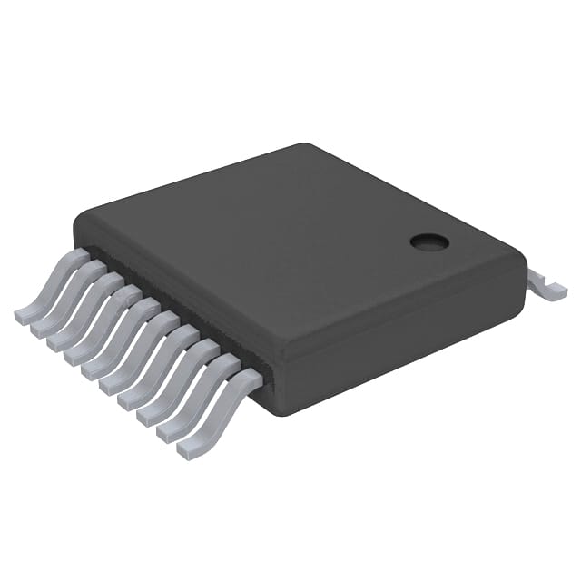
- Package: VSSOP (Very Small Outline Package)
- Essence: A high-performance buffer/line driver IC designed for use in various electronic applications.
- Packaging/Quantity: Available in reels of 2500 units
Specifications
- Supply Voltage Range: 2 V to 5.5 V
- Input Voltage Range: 0 V to VCC
- Output Voltage Range: 0 V to VCC
- Maximum Operating Frequency: 50 MHz
- Number of Buffers/Drivers: 8
- Input/Output Type: Non-Inverting
- Output Current: ±8 mA
- Propagation Delay Time: 6 ns (max)
- Operating Temperature Range: -40°C to +85°C
Detailed Pin Configuration
The SN74AHC540DGVR has a total of 20 pins, which are assigned as follows:
- GND (Ground)
- A1 (Input/Output)
- Y1 (Output)
- A2 (Input/Output)
- Y2 (Output)
- A3 (Input/Output)
- Y3 (Output)
- A4 (Input/Output)
- Y4 (Output)
- A5 (Input/Output)
- Y5 (Output)
- A6 (Input/Output)
- Y6 (Output)
- A7 (Input/Output)
- Y7 (Output)
- A8 (Input/Output)
- Y8 (Output)
- OE (Output Enable)
- VCC (Power Supply)
- GND (Ground)
Functional Features
- High-Speed Operation: The SN74AHC540DGVR is designed to operate at high frequencies, making it suitable for applications requiring fast signal transmission.
- CMOS Logic: This IC utilizes CMOS technology, which provides low power consumption and improved noise immunity.
- Octal Buffer/Line Driver: With eight buffers/drivers, this IC can handle multiple input/output signals simultaneously.
- Non-Inverting: The input and output signals have the same logic polarity, simplifying circuit design.
Advantages and Disadvantages
Advantages: - High-speed operation allows for efficient signal transmission. - CMOS technology ensures low power consumption. - Octal configuration enables handling of multiple signals. - Non-inverting feature simplifies circuit design.
Disadvantages: - Limited output current may not be suitable for driving heavy loads. - Propagation delay time may affect timing-sensitive applications.
Working Principles
The SN74AHC540DGVR operates by receiving input signals on its eight input pins (A1-A8) and providing corresponding output signals on the eight output pins (Y1-Y8). The OE (Output Enable) pin controls the activation of the outputs. When OE is low, the outputs are enabled, allowing the input signals to pass through. Conversely, when OE is high, the outputs are disabled, resulting in a high-impedance state.
Detailed Application Field Plans
The SN74AHC540DGVR finds applications in various electronic systems, including:
- Data Communication: Used as a buffer/line driver in data communication interfaces to ensure reliable signal transmission.
- Memory Systems: Employed in memory modules to amplify and buffer address and data signals.
- Industrial Automation: Integrated into control systems to interface between different components and ensure proper signal levels.
- Automotive Electronics: Utilized in automotive systems for signal buffering and level shifting purposes.
- Consumer Electronics: Incorporated in devices such as televisions, audio systems, and gaming consoles to enhance signal integrity.
Detailed and Complete Alternative Models
- SN74AHC541DGVR: Similar to SN74AHC540DGVR but with tri-state outputs.
- SN74AHCT540DGVR: Compatible alternative with TTL (Transistor-Transistor Logic) input/output levels.
- SN74LVC540ADGVR: Low-voltage alternative with 3.3 V supply voltage range.
These alternative models offer similar functionality and can be used as replacements for the SN74AHC540DGVR in various applications.
Word count: 511 words
Enumere 10 preguntas y respuestas comunes relacionadas con la aplicación de SN74AHC540DGVR en soluciones técnicas
Sure! Here are 10 common questions and answers related to the application of SN74AHC540DGVR in technical solutions:
Question: What is the SN74AHC540DGVR?
Answer: The SN74AHC540DGVR is a non-inverting octal buffer and line driver with 3-state outputs.Question: What is the voltage supply range for the SN74AHC540DGVR?
Answer: The voltage supply range for this device is from 2 V to 5.5 V.Question: What is the maximum output current of the SN74AHC540DGVR?
Answer: The maximum output current per channel is 8 mA.Question: Can the SN74AHC540DGVR be used as a level shifter?
Answer: Yes, it can be used as a level shifter to convert signals between different voltage levels.Question: How many channels does the SN74AHC540DGVR have?
Answer: It has 8 channels, each with a separate input and output.Question: What is the purpose of the 3-state outputs in the SN74AHC540DGVR?
Answer: The 3-state outputs allow multiple devices to share a common bus without interfering with each other.Question: What is the maximum operating frequency of the SN74AHC540DGVR?
Answer: The maximum operating frequency is typically 50 MHz.Question: Can the SN74AHC540DGVR be used in both digital and analog applications?
Answer: No, it is primarily designed for digital applications.Question: Does the SN74AHC540DGVR have built-in protection features?
Answer: Yes, it has built-in ESD protection to prevent damage from electrostatic discharge.Question: What is the package type of the SN74AHC540DGVR?
Answer: It comes in a small SOT-23-6 package, which is suitable for space-constrained applications.
Please note that these answers are general and may vary depending on specific application requirements.