

Consulte las especificaciones para obtener detalles del producto.
SN74AUC34RGYR
Product Overview
- Category: Integrated Circuit (IC)
- Use: Logic Gate
- Characteristics: Low-power, high-speed, 5V tolerant inputs, Schmitt-trigger input
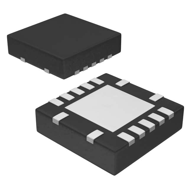
- Package: VQFN-14
- Essence: Hex Buffer/Inverter
- Packaging/Quantity: Tape and Reel, 2500 pieces per reel
Specifications
- Supply Voltage Range: 0.8V to 3.6V
- High-Level Input Voltage: 2V to VCC + 0.3V
- Low-Level Input Voltage: -0.3V to 0.8V
- High-Level Output Voltage: VCC - 0.3V
- Low-Level Output Voltage: 0.3V
- Maximum Operating Frequency: 500MHz
- Propagation Delay: 1.9ns (typical)
Detailed Pin Configuration
The SN74AUC34RGYR has a VQFN-14 package with the following pin configuration:
__    __
   Y1 | 1    14 | VCC
   A1 | 2    13 | Y2
   B1 | 3    12 | A2
   B2 | 4    11 | Y3
   A3 | 5    10 | B3
  GND | 6     9 | B4
   Y4 | 7     8 | A4
       ‾‾    ‾‾
Functional Features
- Hex Buffer/Inverter: The SN74AUC34RGYR consists of six independent buffer/inverter gates. It can be used as a buffer or an inverter depending on the input and output connections.
- Low-Power: The IC is designed to operate at low power, making it suitable for battery-powered devices and energy-efficient applications.
- High-Speed: With a maximum operating frequency of 500MHz, the SN74AUC34RGYR provides fast signal processing capabilities.
- 5V Tolerant Inputs: The IC can tolerate input voltages up to 5V, allowing it to interface with both 3.3V and 5V logic systems.
- Schmitt-Trigger Input: The Schmitt-trigger input ensures robust and noise-immune operation by providing hysteresis.
Advantages and Disadvantages
Advantages: - Low-power consumption - High-speed operation - Wide supply voltage range - 5V tolerant inputs for compatibility - Schmitt-trigger input for noise immunity
Disadvantages: - Limited number of gates (six in total) - VQFN package may require specialized handling during assembly
Working Principles
The SN74AUC34RGYR operates based on the principles of digital logic. It uses CMOS technology to implement the buffer/inverter gates. When an input signal is applied to one of the gates, the IC processes the signal according to its configuration as either a buffer or an inverter. The output signal is then generated based on the input and the gate's functionality.
Detailed Application Field Plans
The SN74AUC34RGYR finds applications in various fields, including:
- Communication Systems: The IC can be used in communication systems for signal conditioning, level shifting, and waveform generation.
- Industrial Automation: It can be employed in industrial automation systems for logic-level conversions and interfacing between different components.
- Consumer Electronics: The IC is suitable for use in consumer electronics such as smartphones, tablets, and wearable devices for signal processing and logic operations.
- Automotive Electronics: It can be utilized in automotive electronics for control systems, sensor interfacing, and signal conditioning.
- Internet of Things (IoT): The IC can be integrated into IoT devices for data processing, control logic, and sensor interfacing.
Detailed and Complete Alternative Models
- SN74AUC34RGYR: The model discussed in this entry.
- SN74LVC04APWR: Hex Inverter with 3.3V to 5V tolerant inputs.
- SN74HC14N: Hex Schmitt-Trigger Inverter with 2V to 6V supply voltage range.
- SN74LV1T34DBVR: Single Buffer/Driver with 1.65V to 5.5V supply voltage range.
- SN74AUP1G34DCKR: Single Buffer/Driver with 0.8V to 3.6V supply voltage range.
(Note: This list is not exhaustive and there are many other alternative models available in the market.)
In conclusion, the SN74AUC34RGYR is a low-power, high-speed hex buffer/inverter IC. It offers 5V tolerant inputs, Sch
Enumere 10 preguntas y respuestas comunes relacionadas con la aplicación de SN74AUC34RGYR en soluciones técnicas
Sure! Here are 10 common questions and answers related to the application of SN74AUC34RGYR in technical solutions:
Q: What is SN74AUC34RGYR? A: SN74AUC34RGYR is a specific model of a hex buffer/inverter integrated circuit (IC) manufactured by Texas Instruments.
Q: What is the purpose of SN74AUC34RGYR? A: SN74AUC34RGYR is used to provide buffering and inversion functions in digital logic circuits.
Q: What voltage levels does SN74AUC34RGYR support? A: SN74AUC34RGYR supports voltage levels ranging from 0.8V to 3.6V, making it compatible with various digital systems.
Q: How many buffers/inverters are there in SN74AUC34RGYR? A: SN74AUC34RGYR consists of six independent buffers/inverters in a single package.
Q: What is the maximum output current of SN74AUC34RGYR? A: The maximum output current per channel of SN74AUC34RGYR is typically around 24mA.
Q: Can SN74AUC34RGYR be used in high-speed applications? A: Yes, SN74AUC34RGYR is designed for high-speed operation and can be used in applications with fast switching requirements.
Q: Is SN74AUC34RGYR suitable for bidirectional data transfer? A: No, SN74AUC34RGYR is unidirectional and can only be used for one-way data transmission.
Q: What is the power supply voltage range for SN74AUC34RGYR? A: The power supply voltage range for SN74AUC34RGYR is typically between 0.8V and 3.6V.
Q: Can SN74AUC34RGYR tolerate overvoltage conditions? A: No, SN74AUC34RGYR is not designed to tolerate overvoltage conditions and may get damaged if subjected to excessive voltages.
Q: What is the package type of SN74AUC34RGYR? A: SN74AUC34RGYR is available in a small-outline integrated circuit (SOIC) package with 14 pins.
Please note that these answers are general and may vary depending on the specific datasheet and application requirements.