

Consulte las especificaciones para obtener detalles del producto.
SN74AUP1G58YZTR
Product Overview
- Category: Integrated Circuit
- Use: Logic Gate
- Characteristics: Single 2-Input Positive OR Gate
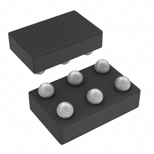
- Package: SOT-23 (5-Pin)
- Essence: High-Speed CMOS Technology
- Packaging/Quantity: Tape and Reel, 3000 pieces per reel
Specifications
- Supply Voltage Range: 0.8V to 3.6V
- Input Voltage Range: -0.5V to VCC + 0.5V
- Output Voltage Range: 0V to VCC
- Maximum Operating Frequency: 500MHz
- Propagation Delay: 2.9ns (typical)
- Low Power Consumption: ICC = 0.9μA (maximum)
Detailed Pin Configuration
The SN74AUP1G58YZTR has the following pin configuration:
```
| | --|1 5|-- --|2 4|-- --|3___| ```
Pin 1: Input A Pin 2: Input B Pin 3: Ground (GND) Pin 4: Output (Y) Pin 5: Power Supply (VCC)
Functional Features
- Performs logical OR operation on two input signals (A and B)
- Provides a single output signal (Y) based on the logical OR result
- Supports high-speed data transmission up to 500MHz
- Works with a wide supply voltage range of 0.8V to 3.6V
- Utilizes low power consumption for energy-efficient operation
Advantages and Disadvantages
Advantages: - High-speed operation allows for efficient data processing - Wide supply voltage range enables compatibility with various systems - Low power consumption reduces energy usage and extends battery life - Small package size (SOT-23) saves board space in compact designs
Disadvantages: - Limited to 2-input OR gate functionality - Not suitable for applications requiring more complex logic operations
Working Principles
The SN74AUP1G58YZTR is based on high-speed CMOS technology. It utilizes transistors and other electronic components to perform the logical OR operation on the input signals (A and B). The internal circuitry processes the inputs and generates the output signal (Y) based on the logical OR result. The gate operates within a specified supply voltage range and provides fast propagation delay, ensuring efficient data processing.
Detailed Application Field Plans
The SN74AUP1G58YZTR can be used in various applications that require logical OR operations, such as:
- Digital Logic Systems: Used to combine multiple input signals and generate a single output based on their logical OR result.
- Data Communication: Enables data routing and switching by performing OR operations on control signals.
- Signal Processing: Utilized in audio and video processing circuits to combine or select different input signals.
- Industrial Automation: Integrated into control systems to process sensor inputs and trigger appropriate actions based on logical conditions.
Detailed and Complete Alternative Models
- SN74AUP1G32YZPR: Single 2-Input Positive OR Gate with Schmitt-Trigger Inputs
- SN74AUP1G08DCKR: Single 2-Input Positive AND Gate
- SN74AUP1G00DRLR: Single 2-Input Positive NAND Gate
- SN74AUP1G125DBVR: Single Bus Buffer Gate with 3-State Outputs
These alternative models provide similar functionality but may have different characteristics, package options, or additional features to suit specific application requirements.
Word count: 430 words
Enumere 10 preguntas y respuestas comunes relacionadas con la aplicación de SN74AUP1G58YZTR en soluciones técnicas
Sure! Here are 10 common questions and answers related to the application of SN74AUP1G58YZTR in technical solutions:
Q1: What is the SN74AUP1G58YZTR? A1: The SN74AUP1G58YZTR is a single 2-input positive-AND gate that operates at a voltage range of 0.8V to 3.6V.
Q2: What are the typical applications of SN74AUP1G58YZTR? A2: It can be used in various applications such as signal conditioning, level shifting, and logic gate interfacing.
Q3: What is the maximum operating frequency of SN74AUP1G58YZTR? A3: The maximum operating frequency of SN74AUP1G58YZTR is typically around 500 MHz.
Q4: What is the input voltage threshold for SN74AUP1G58YZTR? A4: The input voltage threshold for SN74AUP1G58YZTR is typically around 0.7V.
Q5: Can SN74AUP1G58YZTR operate with a supply voltage below 0.8V? A5: No, SN74AUP1G58YZTR requires a minimum supply voltage of 0.8V for proper operation.
Q6: What is the output drive capability of SN74AUP1G58YZTR? A6: SN74AUP1G58YZTR has a typical output drive capability of 32 mA.
Q7: Is SN74AUP1G58YZTR compatible with other logic families? A7: Yes, SN74AUP1G58YZTR is compatible with both CMOS and TTL logic families.
Q8: Does SN74AUP1G58YZTR have built-in protection features? A8: Yes, SN74AUP1G58YZTR has built-in ESD (electrostatic discharge) protection.
Q9: Can SN74AUP1G58YZTR be used in high-temperature environments? A9: Yes, SN74AUP1G58YZTR is designed to operate in a temperature range of -40°C to 125°C.
Q10: What is the package type for SN74AUP1G58YZTR? A10: SN74AUP1G58YZTR is available in a small SOT-23-5 package.
Please note that these answers are general and may vary depending on the specific datasheet and manufacturer's specifications.