

Consulte las especificaciones para obtener detalles del producto.
SN74LVC574AGQNR
Product Overview
- Category: Integrated Circuit (IC)
- Use: Flip-Flop
- Characteristics: Low-voltage, high-speed, octal D-type flip-flop with 3-state outputs
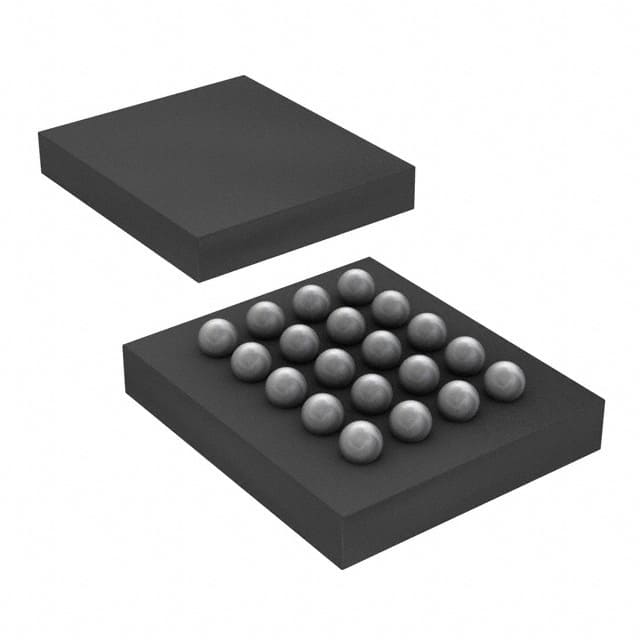
- Package: 20-pin TSSOP package
- Essence: This IC is designed to store and transfer data in electronic circuits.
- Packaging/Quantity: Available in tape and reel packaging, with a quantity of 2500 units per reel.
Specifications
- Supply Voltage Range: 1.65V to 5.5V
- High-Level Input Voltage: 2V to VCC + 0.5V
- Low-Level Input Voltage: -0.5V to 0.8V
- High-Level Output Voltage: 2.4V (min) at IOH = -12mA
- Low-Level Output Voltage: 0.4V (max) at IOL = 24mA
- Operating Temperature Range: -40°C to 85°C
Detailed Pin Configuration
The SN74LVC574AGQNR has a total of 20 pins, which are assigned specific functions as follows:
- GND: Ground pin
- D0: Data input/output pin 0
- D1: Data input/output pin 1
- D2: Data input/output pin 2
- D3: Data input/output pin 3
- D4: Data input/output pin 4
- D5: Data input/output pin 5
- D6: Data input/output pin 6
- D7: Data input/output pin 7
- OE: Output enable input pin
- CP: Clock input pin
- MR: Master reset input pin
- Q0: Flip-flop output pin 0
- Q1: Flip-flop output pin 1
- Q2: Flip-flop output pin 2
- Q3: Flip-flop output pin 3
- Q4: Flip-flop output pin 4
- Q5: Flip-flop output pin 5
- Q6: Flip-flop output pin 6
- Q7: Flip-flop output pin 7
Functional Features
- Octal D-type flip-flop with 3-state outputs
- High-speed operation, suitable for applications requiring fast data transfer
- Low-voltage operation, making it compatible with a wide range of electronic systems
- 3-state outputs allow multiple devices to share the same bus without interference
- Master reset input for clearing all flip-flops simultaneously
- Output enable input for controlling the state of the outputs
Advantages and Disadvantages
Advantages: - High-speed operation enables efficient data transfer - Low-voltage operation makes it versatile for various electronic systems - 3-state outputs facilitate bus sharing in complex circuits - Master reset input allows for easy initialization of flip-flops
Disadvantages: - Limited number of flip-flops (8 in this case) - Not suitable for applications requiring a large number of storage elements
Working Principles
The SN74LVC574AGQNR is an octal D-type flip-flop that stores and transfers data based on clock signals. When the clock input (CP) receives a rising edge, the data present at the D0-D7 inputs is transferred to the corresponding Q0-Q7 outputs. The outputs remain in this state until the next clock cycle.
The master reset input (MR) can be used to clear all flip-flops simultaneously, setting the outputs to a predefined state. The output enable input (OE) controls the state of the outputs, allowing them to be either active or in a high-impedance state.
Detailed Application Field Plans
The SN74LVC574AGQNR is commonly used in various digital systems and applications, including:
- Microcontrollers and microprocessors
- Data storage devices
- Communication systems
- Industrial automation
- Automotive electronics
- Consumer electronics
Its ability to store and transfer data efficiently makes it suitable for applications that require reliable data handling and synchronization.
Detailed and Complete Alternative Models
- SN74LVCH574A: Similar octal D-type flip-flop with 3-state outputs, but operates at a higher voltage range (1.65V to 3.6V).
- SN74LVC374A: Octal D-type flip-flop with 3-state outputs, but in a different package (20-pin SSOP).
- SN74LVC574APW: Octal D-type flip-flop with 3-state outputs, packaged in a 20-pin TSSOP package like the SN74LVC574AGQNR.
These alternative models
Enumere 10 preguntas y respuestas comunes relacionadas con la aplicación de SN74LVC574AGQNR en soluciones técnicas
Sure! Here are 10 common questions and answers related to the application of SN74LVC574AGQNR:
Question: What is the SN74LVC574AGQNR?
- Answer: The SN74LVC574AGQNR is a octal D-type flip-flop with 3-state outputs, designed for low-voltage (2.5V to 3.6V) applications.Question: What is the maximum operating frequency of the SN74LVC574AGQNR?
- Answer: The SN74LVC574AGQNR has a maximum operating frequency of 100 MHz.Question: What is the input voltage range for the SN74LVC574AGQNR?
- Answer: The input voltage range for the SN74LVC574AGQNR is from ground to VCC.Question: How many flip-flops are there in the SN74LVC574AGQNR?
- Answer: The SN74LVC574AGQNR consists of eight individual D-type flip-flops.Question: What is the output drive capability of the SN74LVC574AGQNR?
- Answer: The SN74LVC574AGQNR has a typical output drive capability of ±24 mA.Question: Can the SN74LVC574AGQNR be used in both parallel and serial data transfer applications?
- Answer: Yes, the SN74LVC574AGQNR can be used in both parallel and serial data transfer applications.Question: Does the SN74LVC574AGQNR have internal pull-up or pull-down resistors?
- Answer: No, the SN74LVC574AGQNR does not have internal pull-up or pull-down resistors.Question: What is the power supply voltage range for the SN74LVC574AGQNR?
- Answer: The power supply voltage range for the SN74LVC574AGQNR is from 2.5V to 3.6V.Question: Can the SN74LVC574AGQNR be used in automotive applications?
- Answer: Yes, the SN74LVC574AGQNR is qualified for automotive applications and meets the AEC-Q100 standard.Question: Is the SN74LVC574AGQNR compatible with other logic families?
- Answer: Yes, the SN74LVC574AGQNR is compatible with both 3.3V and 5V logic families.
Please note that these answers are general and may vary depending on the specific application and requirements. It's always recommended to refer to the datasheet and consult with the manufacturer for detailed information.