

Consulte las especificaciones para obtener detalles del producto.
TLC5615IDGKG4
Product Overview
Category
TLC5615IDGKG4 belongs to the category of digital-to-analog converters (DACs).
Use
This product is used to convert digital signals into analog signals, allowing for precise control of voltage levels in various applications.
Characteristics
- High resolution: TLC5615IDGKG4 offers a resolution of 10 bits, providing accurate analog output.
- Low power consumption: This DAC operates at low power, making it suitable for battery-powered devices.
- Fast settling time: The device has a fast settling time, ensuring quick response to changes in input signals.
- Wide operating voltage range: It can operate within a wide voltage range, accommodating different system requirements.
Package and Quantity
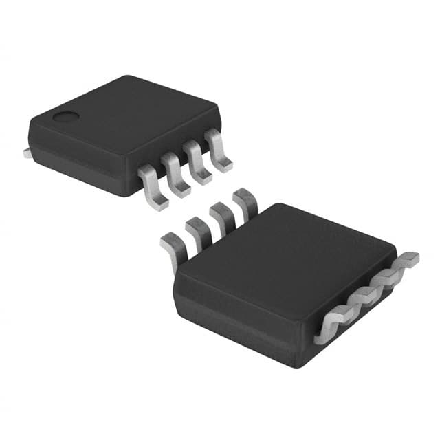
TLC5615IDGKG4 is available in a small form factor package, such as MSOP-8. It is typically sold in reels or tubes containing multiple units.
Specifications
- Resolution: 10 bits
- Supply Voltage Range: 2.7V to 5.5V
- Operating Temperature Range: -40°C to +85°C
- Output Voltage Range: 0V to Vref
- Digital Interface: Serial SPI/I2C
Pin Configuration
The TLC5615IDGKG4 has the following pin configuration:
┌───┬───┐
   │1  └─ 8│
   │        │
   │2      7│
   │        │
   │3      6│
   │        │
   │4      5│
   └───┬───┘
Pin Description: 1. VDD: Power supply voltage 2. CS: Chip select input 3. DIN: Serial data input 4. SCLK: Serial clock input 5. VOUT: Analog output voltage 6. AGND: Analog ground 7. REF: Reference voltage input 8. DGND: Digital ground
Functional Features
- High linearity: TLC5615IDGKG4 provides excellent linearity, ensuring accurate analog output.
- Programmable output range: The output voltage range can be programmed to suit specific application requirements.
- Daisy-chain capability: Multiple devices can be daisy-chained together for simultaneous control.
- Power-down mode: It offers a power-down mode to conserve energy when not in use.
Advantages and Disadvantages
Advantages
- High resolution and accuracy
- Low power consumption
- Fast settling time
- Wide operating voltage range
- Daisy-chain capability
Disadvantages
- Limited output voltage range compared to higher-resolution DACs
- Requires an external reference voltage source
Working Principles
TLC5615IDGKG4 operates based on the digital-to-analog conversion principle. It accepts digital input signals and converts them into corresponding analog voltages. The device utilizes an internal digital-to-analog converter circuitry along with a reference voltage to generate the desired analog output.
Application Field Plans
TLC5615IDGKG4 finds applications in various fields, including but not limited to: 1. Industrial automation: Precise control of analog signals in industrial control systems. 2. Audio equipment: Generation of analog audio signals with high fidelity. 3. Test and measurement instruments: Calibration and signal generation in test setups. 4. Communication systems: Voltage control for RF amplifiers and filters. 5. Automotive electronics: Control of analog signals in automotive systems.
Alternative Models
Other alternative models that offer similar functionality to TLC5615IDGKG4 include: - MCP4921: 12-bit DAC with SPI interface - MAX5216: 16-bit DAC with I2C interface - AD5621: 12-bit DAC with SPI interface
These alternative models can be considered based on specific application requirements and desired resolution.
Word count: 520 words
Enumere 10 preguntas y respuestas comunes relacionadas con la aplicación de TLC5615IDGKG4 en soluciones técnicas
Sure! Here are 10 common questions and answers related to the application of TLC5615IDGKG4 in technical solutions:
Q: What is the TLC5615IDGKG4? A: The TLC5615IDGKG4 is a digital-to-analog converter (DAC) chip that converts digital signals into analog voltage outputs.
Q: What is the resolution of the TLC5615IDGKG4? A: The TLC5615IDGKG4 has a resolution of 10 bits, meaning it can represent 2^10 (1024) different voltage levels.
Q: What is the supply voltage range for the TLC5615IDGKG4? A: The TLC5615IDGKG4 operates with a supply voltage range of 2.7V to 5.5V.
Q: How many channels does the TLC5615IDGKG4 have? A: The TLC5615IDGKG4 is a single-channel DAC, meaning it can generate one analog output voltage at a time.
Q: What is the maximum output voltage range of the TLC5615IDGKG4? A: The TLC5615IDGKG4 can generate an output voltage range from 0V to Vref, where Vref is the reference voltage supplied to the chip.
Q: What is the interface used to communicate with the TLC5615IDGKG4? A: The TLC5615IDGKG4 uses a serial interface, specifically a 3-wire SPI (Serial Peripheral Interface) protocol.
Q: Can the TLC5615IDGKG4 be used in both digital and analog applications? A: Yes, the TLC5615IDGKG4 is commonly used in applications where a digital signal needs to be converted into an analog voltage, such as motor control, audio systems, and instrumentation.
Q: What is the settling time of the TLC5615IDGKG4? A: The settling time refers to the time it takes for the output voltage to stabilize after a change in the digital input. The TLC5615IDGKG4 has a typical settling time of 10µs.
Q: Can the TLC5615IDGKG4 operate in a low-power mode? A: Yes, the TLC5615IDGKG4 has a power-down mode that reduces its power consumption when not in use.
Q: Are there any specific precautions to consider when using the TLC5615IDGKG4? A: It is important to ensure that the reference voltage (Vref) supplied to the TLC5615IDGKG4 is within the specified range and stable. Additionally, proper decoupling capacitors should be used to minimize noise and ensure stable operation.
Please note that these answers are general and may vary depending on the specific application and requirements.