

Consulte las especificaciones para obtener detalles del producto.
TPS61199PWP
Product Overview
Category
The TPS61199PWP belongs to the category of integrated circuits (ICs) and specifically falls under the category of boost converters.
Use
This IC is primarily used for voltage boosting applications, where it efficiently steps up the input voltage to a higher output voltage level.
Characteristics
- High efficiency: The TPS61199PWP offers high conversion efficiency, ensuring minimal power loss during voltage boosting.
- Wide input voltage range: It can accept a wide range of input voltages, making it suitable for various applications.
- Adjustable output voltage: The output voltage can be adjusted according to the specific requirements of the application.
- Protection features: The IC incorporates protection mechanisms such as overvoltage protection and thermal shutdown to safeguard against potential damage.
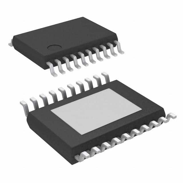
Package
The TPS61199PWP is available in a small outline package (SOP) with a PowerPAD™ thermal pad. This package provides good thermal dissipation and ease of mounting on circuit boards.
Essence
The essence of the TPS61199PWP lies in its ability to efficiently boost input voltages to higher levels while maintaining high conversion efficiency.
Packaging/Quantity
The TPS61199PWP is typically packaged in reels or tubes, containing a specified quantity of ICs per package. The exact packaging and quantity may vary depending on the supplier or manufacturer.
Specifications
- Input Voltage Range: 2.7V to 18V
- Output Voltage Range: Adjustable from 4V to 28V
- Maximum Output Current: 1.5A
- Switching Frequency: Up to 1.2MHz
- Operating Temperature Range: -40°C to +85°C
Detailed Pin Configuration
The TPS61199PWP has the following pin configuration:
- VIN: Input voltage pin
- GND: Ground pin
- FB: Feedback pin for output voltage regulation
- EN: Enable pin to control the IC's operation
- SW: Switching node pin for connecting the inductor
- LX: Inductor connection pin
- VOUT: Output voltage pin
Functional Features
- High Efficiency Conversion: The TPS61199PWP utilizes advanced control techniques to achieve high conversion efficiency, minimizing power loss during voltage boosting.
- Adjustable Output Voltage: The output voltage can be easily adjusted using external resistors or through a feedback mechanism.
- Protection Mechanisms: The IC incorporates overvoltage protection and thermal shutdown features to protect against potential damage caused by excessive voltage or temperature.
- Soft Start: The soft start feature ensures a gradual increase in output voltage during startup, preventing sudden voltage surges.
Advantages and Disadvantages
Advantages
- High conversion efficiency leads to reduced power loss.
- Wide input voltage range allows for versatile applications.
- Adjustable output voltage provides flexibility.
- Protection mechanisms enhance reliability and safety.
- Soft start feature prevents voltage surges during startup.
Disadvantages
- Limited maximum output current of 1.5A may not be suitable for high-power applications.
- Higher switching frequency may require careful consideration of noise interference.
Working Principles
The TPS61199PWP operates as a boost converter, utilizing a switching regulator topology. It converts the input voltage to a higher output voltage level by controlling the duty cycle of the internal switch. This switching action, along with the inductor and capacitor, stores and releases energy to efficiently step up the voltage.
Detailed Application Field Plans
The TPS61199PWP finds applications in various fields, including but not limited to: - Portable electronic devices: Used to power displays, backlighting systems, and other components requiring higher voltages. - Automotive electronics: Suitable for voltage boosting in automotive lighting systems, infotainment displays, and other applications. - Industrial equipment: Used in power supply circuits for industrial control systems, instrumentation, and automation devices.
Detailed and Complete Alternative Models
- TPS61198PWP: Similar to the TPS61199PWP, but with a lower maximum output current of 1A.
- TPS61197PWP: Offers similar features as the TPS61199PWP, but with a different pin configuration.
- TPS61196PWP: A lower-power alternative with a maximum output current of 500mA.
These alternative models provide options with varying specifications and capabilities, allowing designers to choose the most suitable IC for their specific requirements.
Word count: 623 words
Enumere 10 preguntas y respuestas comunes relacionadas con la aplicación de TPS61199PWP en soluciones técnicas
Sure! Here are 10 common questions and answers related to the application of TPS61199PWP in technical solutions:
Q: What is TPS61199PWP? A: TPS61199PWP is a boost converter integrated circuit (IC) that provides a regulated output voltage from a lower input voltage.
Q: What is the typical input voltage range for TPS61199PWP? A: The typical input voltage range for TPS61199PWP is between 2.7V and 18V.
Q: What is the maximum output current that TPS61199PWP can handle? A: TPS61199PWP can handle a maximum output current of 1.5A.
Q: Can TPS61199PWP be used in battery-powered applications? A: Yes, TPS61199PWP can be used in battery-powered applications as it has a wide input voltage range and low quiescent current.
Q: Does TPS61199PWP have built-in protection features? A: Yes, TPS61199PWP has built-in protection features such as overvoltage protection, thermal shutdown, and short-circuit protection.
Q: What is the efficiency of TPS61199PWP? A: The efficiency of TPS61199PWP can reach up to 90% depending on the input and output voltage conditions.
Q: Can TPS61199PWP be used in automotive applications? A: Yes, TPS61199PWP is suitable for automotive applications as it can operate within the required temperature range and has automotive-grade certifications.
Q: How can I control the output voltage of TPS61199PWP? A: The output voltage of TPS61199PWP can be controlled using an external resistor connected to the feedback pin.
Q: Can TPS61199PWP operate in a wide temperature range? A: Yes, TPS61199PWP can operate in a wide temperature range from -40°C to 125°C.
Q: What are some typical applications of TPS61199PWP? A: Some typical applications of TPS61199PWP include LED backlighting for LCD displays, portable devices, automotive lighting, and general-purpose boost converters.
Please note that these answers are general and may vary depending on specific design requirements and datasheet specifications.