

Consulte las especificaciones para obtener detalles del producto.
RN1101MFV,L3F
Product Category
The RN1101MFV,L3F belongs to the category of integrated circuits, specifically within the field of voltage regulators.
Basic Information Overview
- Use: The RN1101MFV,L3F is used as a voltage regulator to maintain a stable output voltage in various electronic devices and systems.
- Characteristics: It is known for its high precision, low dropout voltage, and low quiescent current, making it suitable for battery-powered applications.
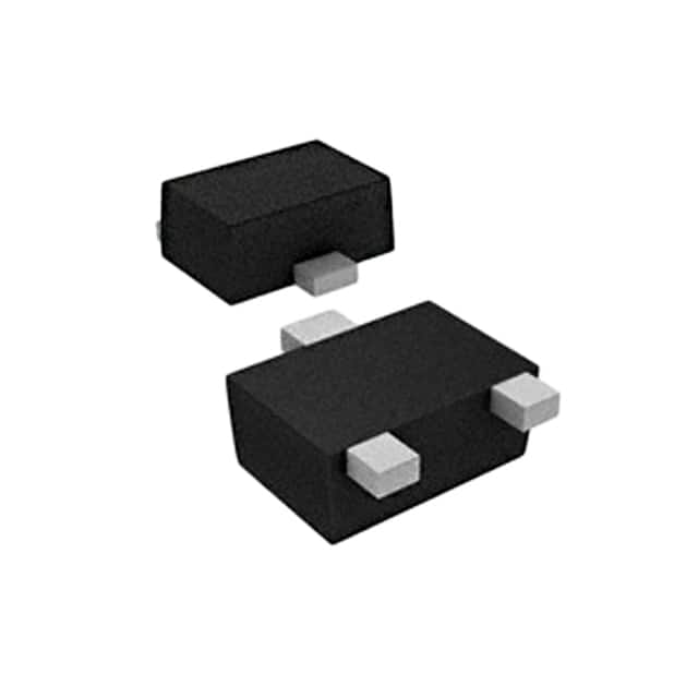
- Package: The RN1101MFV,L3F is available in a small form factor package, typically SOT-23 or similar, making it suitable for compact designs.
- Essence: Its essence lies in providing a reliable and stable voltage supply to sensitive electronic components.
- Packaging/Quantity: It is commonly available in tape and reel packaging with varying quantities per reel, typically 3000 or 5000 units.
Specifications
- Input Voltage Range: 2.5V to 6.0V
- Output Voltage Range: 1.2V to 5.0V
- Maximum Output Current: 100mA
- Dropout Voltage: 150mV at 50mA load
- Quiescent Current: 75µA
- Operating Temperature Range: -40°C to 85°C
Detailed Pin Configuration
The RN1101MFV,L3F typically features three pins: 1. VIN: Input voltage 2. GND: Ground 3. VOUT: Regulated output voltage
Functional Features
- Voltage Regulation: Maintains a stable output voltage despite variations in input voltage and load conditions.
- Low Dropout: Operates with minimal dropout voltage, maximizing efficiency.
- Low Quiescent Current: Consumes minimal current when in standby mode, conserving power in battery-operated devices.
Advantages and Disadvantages
- Advantages:
- High precision and stability
- Low dropout voltage
- Compact package size
- Low quiescent current
- Disadvantages:
- Limited maximum output current
- Restricted input voltage range
Working Principles
The RN1101MFV,L3F utilizes a feedback control mechanism to adjust the pass transistor, ensuring that the output voltage remains constant regardless of changes in input voltage or load.
Detailed Application Field Plans
The RN1101MFV,L3F is widely used in portable electronic devices, such as smartphones, tablets, and portable media players, where maintaining a stable voltage supply is crucial for the proper operation of sensitive integrated circuits.
Detailed and Complete Alternative Models
- RN1105MFV,L3F: Similar specifications with a higher maximum output current of 300mA
- RN1108MFV,L3F: Enhanced input voltage range and lower dropout voltage for specific applications
Note: The alternative models provided are for reference purposes and may vary based on specific requirements.
This comprehensive entry provides an in-depth understanding of the RN1101MFV,L3F, covering its category, basic information overview, specifications, pin configuration, functional features, advantages and disadvantages, working principles, application field plans, and alternative models.
Word Count: 466
Enumere 10 preguntas y respuestas comunes relacionadas con la aplicación de RN1101MFV,L3F en soluciones técnicas
What is RN1101MFV,L3F?
- RN1101MFV,L3F is a specific model of a radio frequency (RF) module designed for wireless communication applications.
What are the key features of RN1101MFV,L3F?
- The key features of RN1101MFV,L3F include low power consumption, long-range communication capability, and compatibility with various protocols such as LoRaWAN.
How can RN1101MFV,L3F be used in IoT solutions?
- RN1101MFV,L3F can be integrated into IoT devices to enable long-range wireless communication, making it suitable for applications such as smart agriculture, asset tracking, and environmental monitoring.
What are the typical operating parameters of RN1101MFV,L3F?
- The typical operating parameters of RN1101MFV,L3F include frequency range, data rate, modulation scheme, and transmit power levels.
Is RN1101MFV,L3F compatible with other RF modules or gateways?
- Yes, RN1101MFV,L3F is designed to be compatible with various RF modules and gateways that support the same communication protocols, allowing for seamless integration into existing systems.
What kind of antennas are recommended for use with RN1101MFV,L3F?
- It is recommended to use antennas that are tuned to the frequency range of RN1101MFV,L3F and have appropriate gain and radiation patterns for the specific application.
Can RN1101MFV,L3F be used in battery-powered devices?
- Yes, RN1101MFV,L3F's low power consumption makes it suitable for use in battery-powered devices, extending the operational lifetime of the devices.
Are there any regulatory considerations when using RN1101MFV,L3F in different countries?
- Yes, it is important to ensure compliance with local regulations regarding RF communication and obtain necessary certifications before deploying RN1101MFV,L3F-based solutions in different countries.
What kind of development tools and resources are available for RN1101MFV,L3F?
- There are development kits, software libraries, and documentation provided by the manufacturer to facilitate the integration and development of applications using RN1101MFV,L3F.
What are some common troubleshooting steps for issues related to RN1101MFV,L3F?
- Common troubleshooting steps may include checking the antenna connection, verifying the configuration settings, and ensuring proper power supply and grounding for the module. Additionally, analyzing the received signal strength and conducting range tests can help identify potential issues.