

Consulte las especificaciones para obtener detalles del producto.
TC7WPB8306L8X,LF
Basic Information Overview
- Category: Integrated Circuit (IC)
- Use: Logic Gate
- Characteristics:
- Low-power consumption
- High-speed operation
- Wide operating voltage range
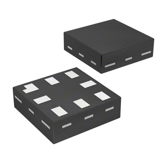
- Package: SOT-353 (5-pin package)
- Essence: N-channel MOSFET logic gate
- Packaging/Quantity: Tape and Reel, 3000 units per reel
Specifications
- Supply Voltage Range: 1.65V to 5.5V
- Input Voltage Range: 0V to VDD
- Output Voltage Range: 0V to VDD
- Operating Temperature Range: -40°C to +85°C
- Propagation Delay Time: 2.5ns (typical)
- Input Capacitance: 3pF (typical)
- Output Capacitance: 4pF (typical)
Detailed Pin Configuration
The TC7WPB8306L8X,LF has the following pin configuration:
```
| | --|1 5|-- --|2 4|-- |____| GND ```
Pin Description: 1. A: Input A 2. B: Input B 3. NC: No Connection 4. Y: Output 5. VDD: Power Supply
Functional Features
- Performs logical AND function on inputs A and B
- Provides a high-level output when both inputs are high
- Supports a wide range of supply voltages
- Low power consumption makes it suitable for battery-powered devices
- High-speed operation enables efficient data processing
Advantages
- Low power consumption extends battery life in portable devices
- High-speed operation allows for quick data processing
- Wide operating voltage range provides flexibility in various applications
- Small package size saves board space
- Reliable performance in a wide temperature range
Disadvantages
- Limited number of inputs (only two)
- Output is active high, which may not be suitable for all applications
- Not suitable for high-current applications due to its small package size
Working Principles
The TC7WPB8306L8X,LF is an N-channel MOSFET logic gate that performs the logical AND function. It consists of two input transistors and one output transistor. When both input A and input B are high, the output Y is driven to a high level. Otherwise, the output remains low.
Detailed Application Field Plans
The TC7WPB8306L8X,LF can be used in various applications, including: 1. Digital signal processing systems 2. Microcontrollers and microprocessors 3. Communication devices 4. Battery-powered devices 5. Industrial automation systems
Detailed and Complete Alternative Models
Some alternative models that can be considered as replacements for the TC7WPB8306L8X,LF include: 1. SN74LVC1G08DBVR - Single 2-Input Positive-AND Gate 2. CD4081BE - Quad 2-Input AND Gate 3. MC14081BCP - Quad 2-Input AND Gate 4. 74HC08N - Quad 2-Input AND Gate
These alternative models offer similar functionality and can be used as substitutes based on specific requirements.
Word count: 346 words
Enumere 10 preguntas y respuestas comunes relacionadas con la aplicación de TC7WPB8306L8X,LF en soluciones técnicas
Sure! Here are 10 common questions and answers related to the application of TC7WPB8306L8X,LF in technical solutions:
1. What is TC7WPB8306L8X,LF? - TC7WPB8306L8X,LF is a specific model of a logic gate IC (integrated circuit) manufactured by Toshiba.
2. What is the function of TC7WPB8306L8X,LF? - TC7WPB8306L8X,LF is a triple 2-input AND gate that performs logical AND operations on two input signals.
3. What voltage levels does TC7WPB8306L8X,LF support? - TC7WPB8306L8X,LF supports a wide range of voltage levels, typically from 2V to 5.5V.
4. Can TC7WPB8306L8X,LF be used in both digital and analog circuits? - No, TC7WPB8306L8X,LF is specifically designed for digital circuits and is not suitable for analog applications.
5. What is the maximum operating frequency of TC7WPB8306L8X,LF? - The maximum operating frequency of TC7WPB8306L8X,LF is typically around 100 MHz.
6. How many gates are there in TC7WPB8306L8X,LF? - TC7WPB8306L8X,LF consists of three independent AND gates in a single package.
7. Can TC7WPB8306L8X,LF be used in high-speed applications? - Yes, TC7WPB8306L8X,LF is suitable for high-speed applications due to its fast propagation delay and transition times.
8. What is the power supply requirement for TC7WPB8306L8X,LF? - TC7WPB8306L8X,LF requires a power supply voltage between 2V and 5.5V.
9. Is TC7WPB8306L8X,LF compatible with other logic families? - Yes, TC7WPB8306L8X,LF is compatible with various logic families such as TTL (Transistor-Transistor Logic) and CMOS (Complementary Metal-Oxide-Semiconductor).
10. Can TC7WPB8306L8X,LF be used in battery-powered devices? - Yes, TC7WPB8306L8X,LF can be used in battery-powered devices as it operates within a wide range of voltage levels and has low power consumption.
Please note that the answers provided here are general and may vary depending on specific application requirements.